Acquiring High-Quality Images Through Silicon Without Damaging the Finished Product
Olympus's UIS2 series of dedicated IR objective lenses offer a turnkey solution for near-IR digital imaging
14 Aug 2018
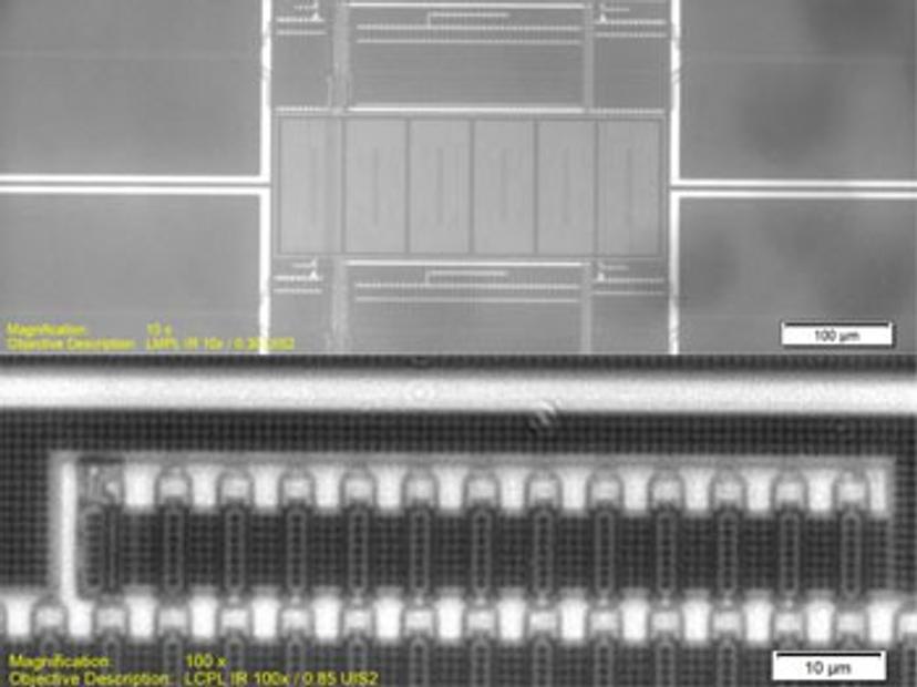
The typical failure-analysis protocol for microelectronics requires the ability to nondestructively inspect circuit patterns through silicon while maintaining the mechanical integrity of the finished product. Noninvasive techniques, such as microscopic imaging in the near-IR spectrum, provide inspection directly through silicon up to 650 μm thick. Applications include inspecting for short circuits within a product (burnout marks, stress indicators, etc.), bonding alignment (analysis of alignment marks between thinly bonded circuits), inspection after electrical testing (any type of failure), and chip damage (defects in materials, contamination, etc.).
The requirements by most failure-analysis and R&D laboratories for measuring defects, creating reports, and archiving images demand a digital solution. Due to the inherent nature of this application, native contrast is minimal and must be optimized through image analysis software. The function of the non-uniformity of the illumination creates vignetting or darkening of the image corners to the center and must be digitally removed from the live view and captured image. While reflected light microscopy is ideal for illuminating a sample from above, transmitted light IR is designed to bring light to a sample through silicon from beneath the sample, providing higher contrast. This allows transmitted light to be especially useful for the inspection of pattern alignment or fiducial marks through silicon.
A Complete Digital Near-IR System
Olympus's UIS2 series of dedicated IR objective lenses offer a turnkey solution for near-IR digital imaging, providing increased transmittance at the near-IR spectrum and provide correction collars (20x, 50x, and 100x objective lenses) to be set for a specific silicon thickness, maximizing transmittance and performance. The Olympus XM10-IR digital camera provides high-contrast images throughout the near-IR spectrum up to 1100 nm while still maintaining a large field of view thanks to the large 2/3 in. CCD sensor. OLYMPUS Stream® image analysis software fully controls the XM10-IR camera, unlike other IR imaging solutions, to provide live shading correction to maximize image uniformity across the field of view. Furthermore, the user can easily maximize image contrast on both live and captured IR images. OLYMPUS Stream software also provides the ability to perform accurate measurements anywhere within the image field of view, automatically create reports, and archive images and relevant data.
Ideal for high-quality imaging and inspection through silicon, Olympus's complete digital near-IR solution includes:
- Upright IR compound microscope (BX series) or dedicated IR wafer inspection compound microscope (MX series) (MX series IR microscopes enable simultaneous reflected light and transmitted light IR observation)
- UIS2-IR objective lenses
- XM10-IR high-sensitivity 1.4 MP CCD digital FireWire camera
- OLYMPUS Stream image analysis software
- Start Getting Results Immediately
Olympus's turnkey digital near-IR system provides the ability to acquire high-quality images beneath silicon, perform accurate measurements, create compelling reports, and archive images, all without damaging the finished product. In addition, by utilizing a digital near-IR sensor, the characteristic image lag and retention of an analog lead sulfide tube camera is eliminated. This complete solution is also user-friendly—operators with a basic understanding of microscopy and imaging can start attaining results immediately.