Argon Ion Polishing of Focused Ion Beam Specimens in PIPS II System
By Anahita Pakzad, Gatan, Inc.
13 Jan 2016
As researchers push boundaries of elemental analysis and HR imaging with their transmission electron microscope (TEM), ultra-low damage specimens less than 40 nm thickness are frequently required. When evaluating preparation techniques for these thin lamellae, it is important to consider class of material being polished and whether the method is reproducible when applied across multiple samples. Here we will discuss broad argon (Ar) beam ion milling and focused ion beam milling (FIB). These two most common techniques are used for preparation of electron transparent specimens for a diverse class of materials, including semiconductors, metals and ceramics.
When assessing techniques, FIB is especially viable when specific sample orientation or site specific positional accuracy is required. However, amorphization, implantation and vacancies due to application of high energy gallium (Ga) ions, sample alteration due to beam heating in addition to re-deposition, surface roughness and selective abrasion are some of various damages caused by this method.1
Amongst these problems, FIB-induced surface amorphization is the most extensive and limiting as it reduces the signal-to-noise ratio.2 Additionally in order to avoid geometrical blurring for high resolution transmission electron microcopy (HRTEM) applications, sample thickness must be reduced by the square root of the feature size.3 A 25 keV Ga+ FIB column can generate ~20 nm per specimen side damage in silicon (Si).4 This can be specifically limiting in modern Si-based semiconductor devices, where minimum feature size is less than 20 nm.
The depth of FIB induced amorphous layer depends on beam energy, beam angle and material being milled, different techniques commonly used to reduce this damage in TEM samples are:
- Gas-assisted etching: Method enhances the milling rate, however increases roughness of crystalline- amorphous interface that further damages TEM images5
- Low-energy FIB: Reduction of beam energy minimizes damage depth, although etching rate and positional resolution are also impacted at these energies
- Wet etching: Single layered materials benefit significantly when used with suitable solution3, but because of different etching rates, this method cannot be used for multi-layer semiconductor devices
- Argon ion milling: Most promising method for multi-layer materials, as none of the drawbacks mentioned above is present. Here the original FIB damage layer is replaced by newly formed Ar ion- induced damage layer.3,6 The thickness of this layer depends on the milling energy, angle and time, which are all parameters controlled by the user in the PIPS™ II system
Practical Aspects of Argon Ion Polishing of Fib Specimens in Pips II System
As mentioned above, to optimize new layer thickness formed during Ar polishing of FIB-induced amorphous layer, while avoiding re-deposition or specimen contamination, several parameters should be considered:
Beam energy: Low energy ions have shallow penetration depth that reduces ion-induced surface damage. For final polishing steps, beam energies lower than 300 eV are recommended.
Milling time: Because the Ar ion beam is well focused at low energies in the PIPS II System (~1 mm FWHM), current density at the milling area is high, thus material removal rate is high. Optimize milling time to remove enough material to improve sample quality, but not over-thin the specimen. We recommend milling the specimen for a few tens of second (<60 s), examining it in the microscope, then milling further if required.
Milling angle: Although it is known that a higher beam angle increases the ion induced surface damage, at low beam energies, commonly used for this specific application (<0.5 keV), stopping and range of ions in matter (SRIM) models show that the sputtering yields are very similar at high and low angles. For post-FIB polishing in PIPS II system, higher angles are best applied, while considering any constraints from the mounting grid geometry. Milling both from top and bottom reduces the chances of the thin areas generating bending of the lamella.
- Sample temperature: To prevent heat-induced damage caused by ion bombardment, the stage (specimen) temperature is reduced to ensure the milling area remains close to ambient temperature while milling
- Ion milling mode: Due to the size and geometry of the thin lamellae inside the PIPS chamber, we have found that keeping the sample stationary and milling with only one gun at a time provides the best results and the least amount of re-deposition (PIPS II Stationary milling mode)
- Type of supporting grid: Molybdenum (Mo) and Copper (Cu) are the two most common grid materials. Mo has a lower sputtering rate that reduces the chance of re-deposition from grid onto the FIB lamella
- Position of FIB thinned area with respect to the milling gun: FIB specimens are either H-bars, or lift-out type (mounted on a grid fingertip or side wall)
- After mounting in the DuoPost®, place the sample at the PIPS II Home Position as shown in Figure 1c
- Bring the thin lamella to center of rotation using the touch screen alignment page and X,Y stage movement available on the PIPS II system
- To reduce re-deposition, orient the stage rotation angle so the ion beam passes over the lamella before milling the substrate or grid
- For lift-out specimens mounted on the grid finger’s side wall, rotate the PIPS II stage about 5º offset from the pre-set positions in the alignment page (Figure 2)
- While selecting this offset angle, note the Ar beam is about 1 mm wide and is not as small as the lamella
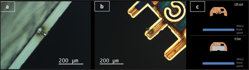
Figure 1. PIPS II optical images of: (a) FIB H-bar sample and (b) FIB lift-out specimen mounted on the side wall of a Cu grid. (c) Top view cartoons show samples in home position as they are inserted in PIPS II system for post FIB polish.
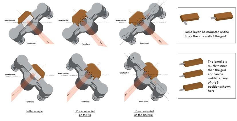
Figure 2. Illustrations show how FIB H-bar and lift-out specimens are oriented with respect to the left and right guns. When lamella is mounted on the side wall of a grid finger, it is better to rotate the specimen at least 5º offset, so the beam does not deposit grid/substrate or weld material on the specimen thin area. Note that as shown in images on the right, the thickness of the lamella is much less than the grid, as a result the lamella can be welded at different positions on the finger.
Results
In these examples, the quality of FIB-prepared TEM samples improved and the FIB induced amorphous layer thickness reduced by application of low energy (<300 eV), broad beam ion milling in the PIPS II system. This improvement occurred without depositing holder or grid material onto the polished thin area.
When using lift-out samples, they were mounted on either Cu or Mo OmniProbe grids. Specimens were imaged before polishing in the PIPS II System as reference of the sample condition after preparation in FIB. Samples were then polished using low energy Ar ion guns in stages with sequential observation in a TEM. Argon beams were set to mill at incident angles >7° from either top or bottom. The lamellae were centered using the PIPS II X,Y stage, aligned with respect to each gun, then milled using Stationary milling mode. Samples were cooled during polishing to reduce heat induced damage (-80 ºC).
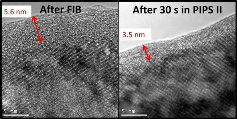
Figure 3: Removal of FIB produced amorphous surface layers in a Niobium (Nb) sample can be readily seen in these micrographs. The right image shows changes after 30 s of milling at 300 eV. During this time, the amorphous layer was reduced from approximately 5.6 to 3.5 nm (~40% reduction). FIB prepared specimen provided by University of Chicago, Illinois.
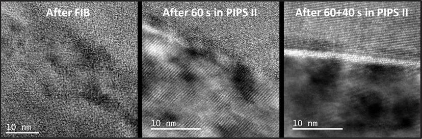
Figure 4. TEM micrographs of a multi-layer sample as prepared in FIB (left), after polishing in PIPS II System at 300 eV for 60 s (center), after polishing in PIPS II system for additional 40 s (right). Due to FIB-induced amorphization, the second layer in the middle is not visible in the first two images (left and center), but after sufficient Ar ion polishing it is clearly visible in the last one (right). FIB prepared specimen provided by Texas Instruments, Dallas Texas.
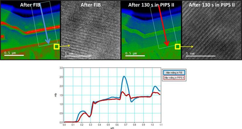
Figure 5. Color images (left) show sample thickness maps* in the device, captured after milling in FIB (H-bar) and low energy milling in PIPS II system (300 eV beam, stationary milling mode, 130 s). Sample thickness is compared in these two images using profile lines averaged along the graph arrows shown below. TEM micrographs (right) show high resolution images taken before and after low energy ion milling in PIPS II system (taken from yellow square areas shown on the thickness maps). By reducing sample thickness, parts of FIB-induced sample surface damage have been removed. FIB prepared specimen provided by Texas Instruments, Dallas Texas. *Rainbow color scale on the thickness maps varies from 0 (black) to 4 (white) mfp.
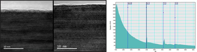
Figure 6. TEM micrographs of a multi-layer sample. The left image was captured as prepared in FIB. The right image was taken after polishing in PIPS II system for 90 s. Due to FIB-induced amorphization, and sample thickness, layers are not clearly visible in the first image, however after Ar ion polishing they are clearly visible. The EELS data (right) shows no sign of re-deposition of grid material (Mo) on the sample.
Conclusions
New features including focused ion beams at low energies (~1 mm in diameter), X,Y alignment stage, optical camera along with DigitalMicrograph® imaging software, stationary milling and custom milling angles in PIPS II system made it possible to polish FIB samples efficiently at <300 eV that improved the sample quality without re-deposition of holder material (Al) or the grid (Cu or Mo).
Thank you to Gatan for this article
References
J. Ayache et al in: ”Sample Preparation Handbook for Transmission Electron Microscopy: Methodology”, (Springer, New York) p. 126.
M.J. Suss, E Mueller and R. Wepf, Ultramicroscopy 111 (2011), p. 1224.
N.I. Kato, Journal of Electron Microscopy 53 (2004), p. 451.
L.A. Giannuzzi and F.A. Stevie, Micron, 30, (1999) p. 197.
K Gamo, Materials Research Society Symposium Proceedings (1993) p. 577.
A Barna, Journal of Computer Assisted Microscopy, 9, (1997), p. 101.