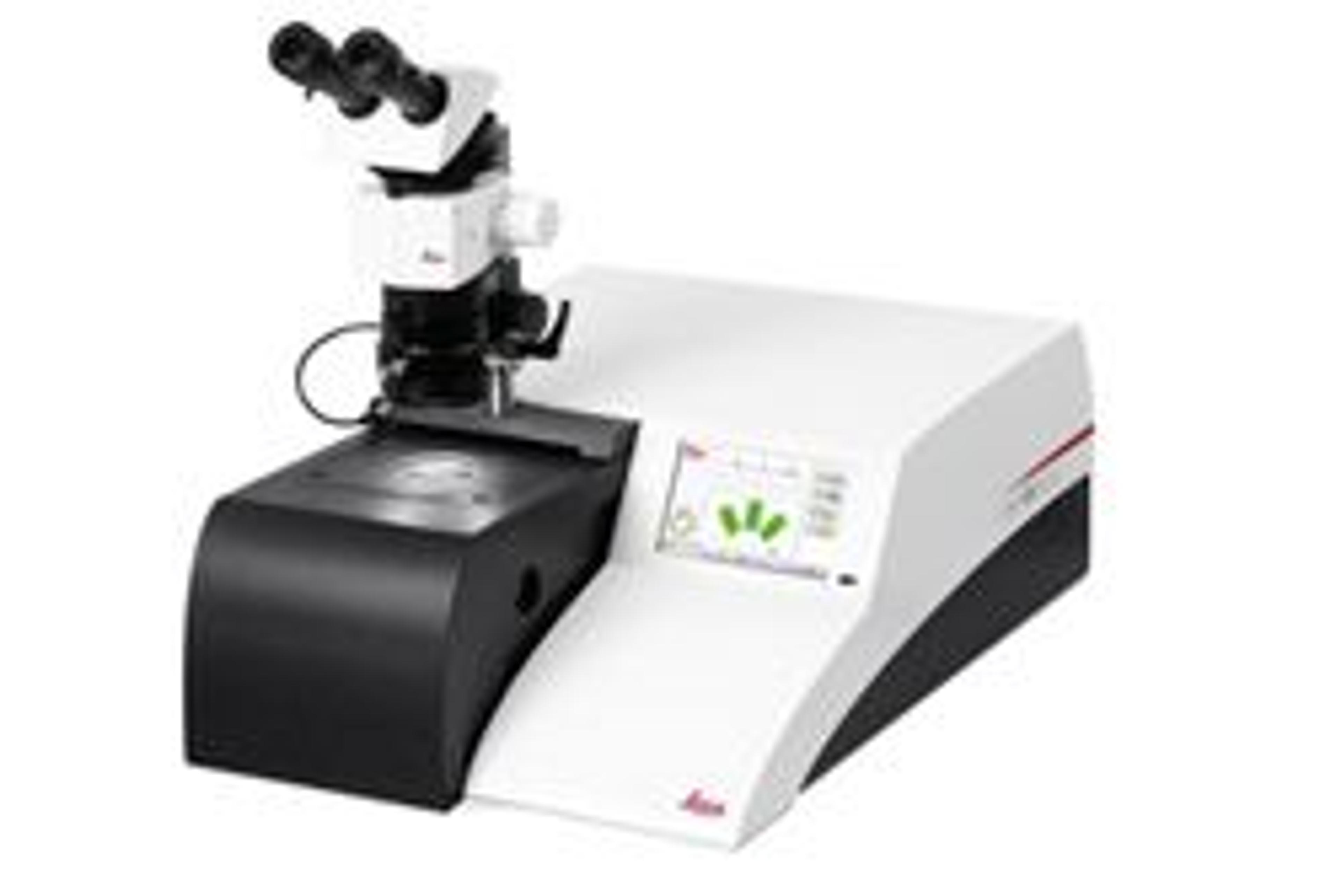
Leica Microsystems’ Ion Beam Milling System Leica EM TIC 3X Now Available With Vacuum Cryo Transfer Docking Port
21 Nov 2014Leica Microsystems’ ion beam milling system Leica EM TIC 3X is now available with a docking port for vacuum cryo transfer. This docking port enables transfer at vacuum and / or cryo conditions with the Leica EM VCT100 vacuum cryo transfer system. Room-temperature or cryo sections can be taken up directly from the ion beam milling system, loaded into the vacuum cryo transfer system, and transferred to the next preparation step.
“The vacuum cryo transfer docking port makes users’ work easier. We offer a perfect setup for surfacing environmentally and cryogenically sensitive samples. With the Leica EM VCT100, researchers can transfer their cross-sections from the ion beam milling system to coating, and on to scanning electron microscopes under innert gas / vacuum conditions as required by the sample. This keeps the sample safe and helps users obtain brilliant images”, says Robert Ranner, Product Manager Leica Microsystems.
In electron microscopy sample preparation, Leica Microsystems focuses on workflow solutions. The vacuum cryo transfer docking port on the Leica EM TIC 3X facilitates this workflow as it provides transfer options for all kinds of samples. “We want to make researchers’ lives easier. One example: Lithium needs to remain in a protective environment during the preparation cycle,” explains Ranner. “Users can now rely on a system that works seamlessly without interruption: The sample is prepared mechanically with the Leica EM TXP target preparation device, cross-sectioned with the Leica EM TIC 3X ion beam milling system, coated in the high vacuum coater Leica EM ACE600 and imaged in the scanning electron microscope. The transport system Leica EM VCT100 serves as a shuttle from one step to the next, always preserving cryo and / or vaccum conditions.”
The ion beam milling system Leica EM TIC 3X is designed to provide users with high quality surface preparation of hard, soft, porous, heat-sensitive, brittle and / or heterogeneous material for microstructure analysis by means of scanning electron microscopy (SEM) and Atomic Force Microscopy (AFM). The prepared sample surface enable researchers to investigate with different techniques such as Energy Dispersive Spectrometry (EDS), Wavelength Dispersive Spectroscopy (WDS), Auger Electron Spectroscopy, or Electron Backscatter Diffraction (EBSD).

