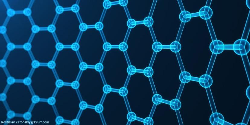
Graphene and other 2D materials are undoubtedly hot topics in the scientific community. With an increasing number of developments in areas of analysis, characterization and research over recent months, the likelihood of delivering on the promise shown by these materials is growing. From the development of a dedicated graphene characterization service for industry to integrated analysis techniques, SelectScience® brings together all the latest news, application notes and videos relevant to the graphene and 2D materials community.
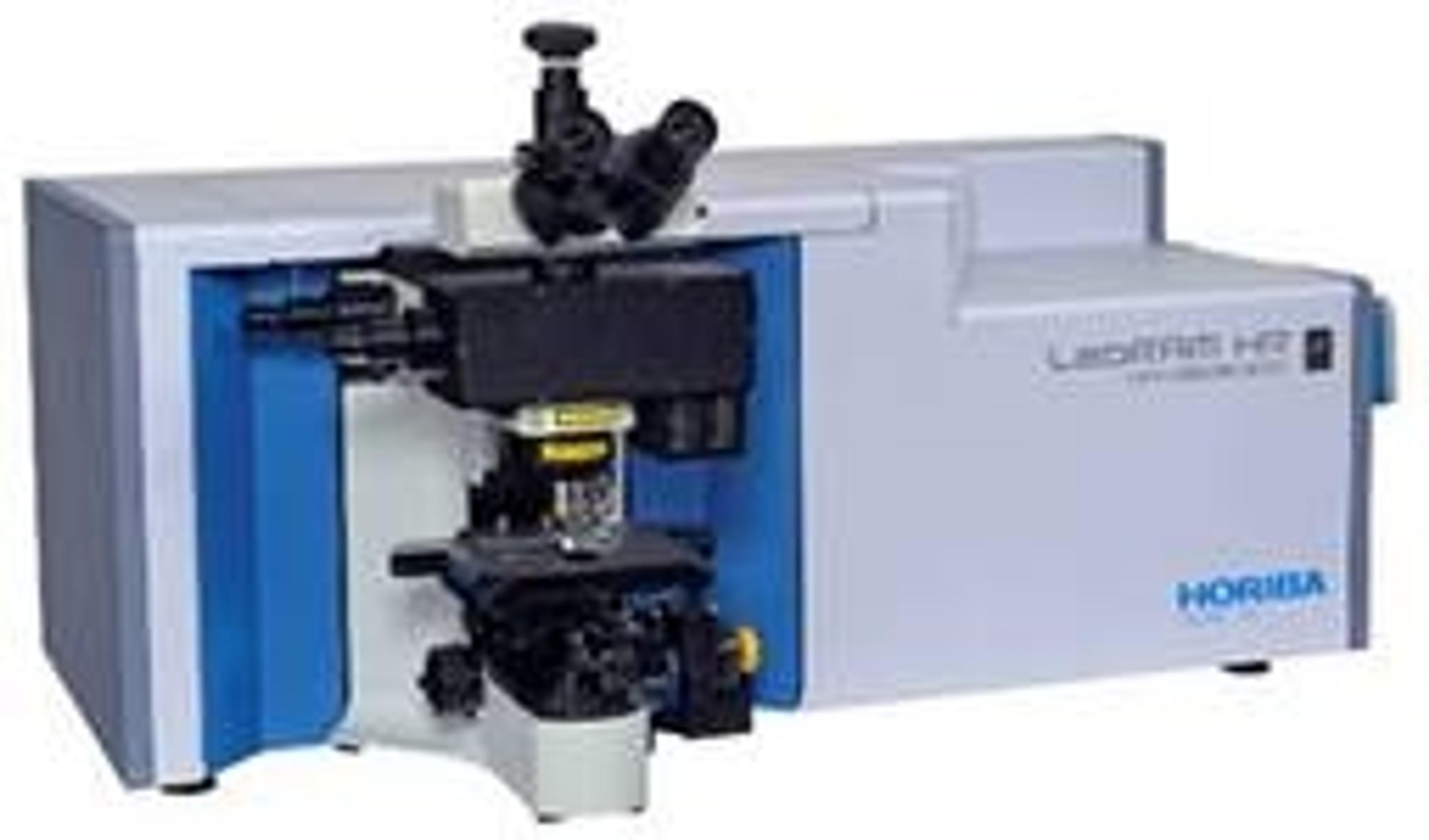
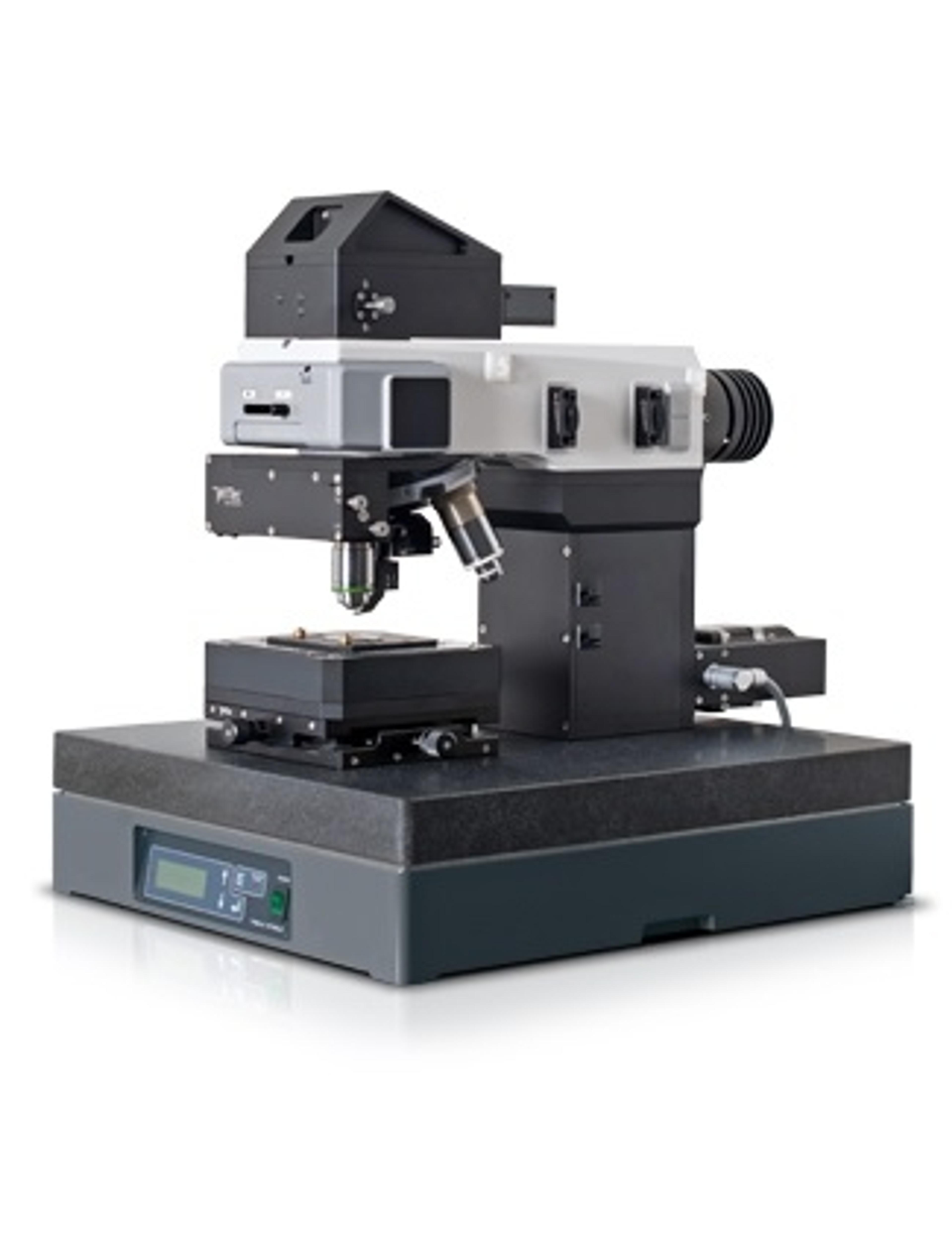
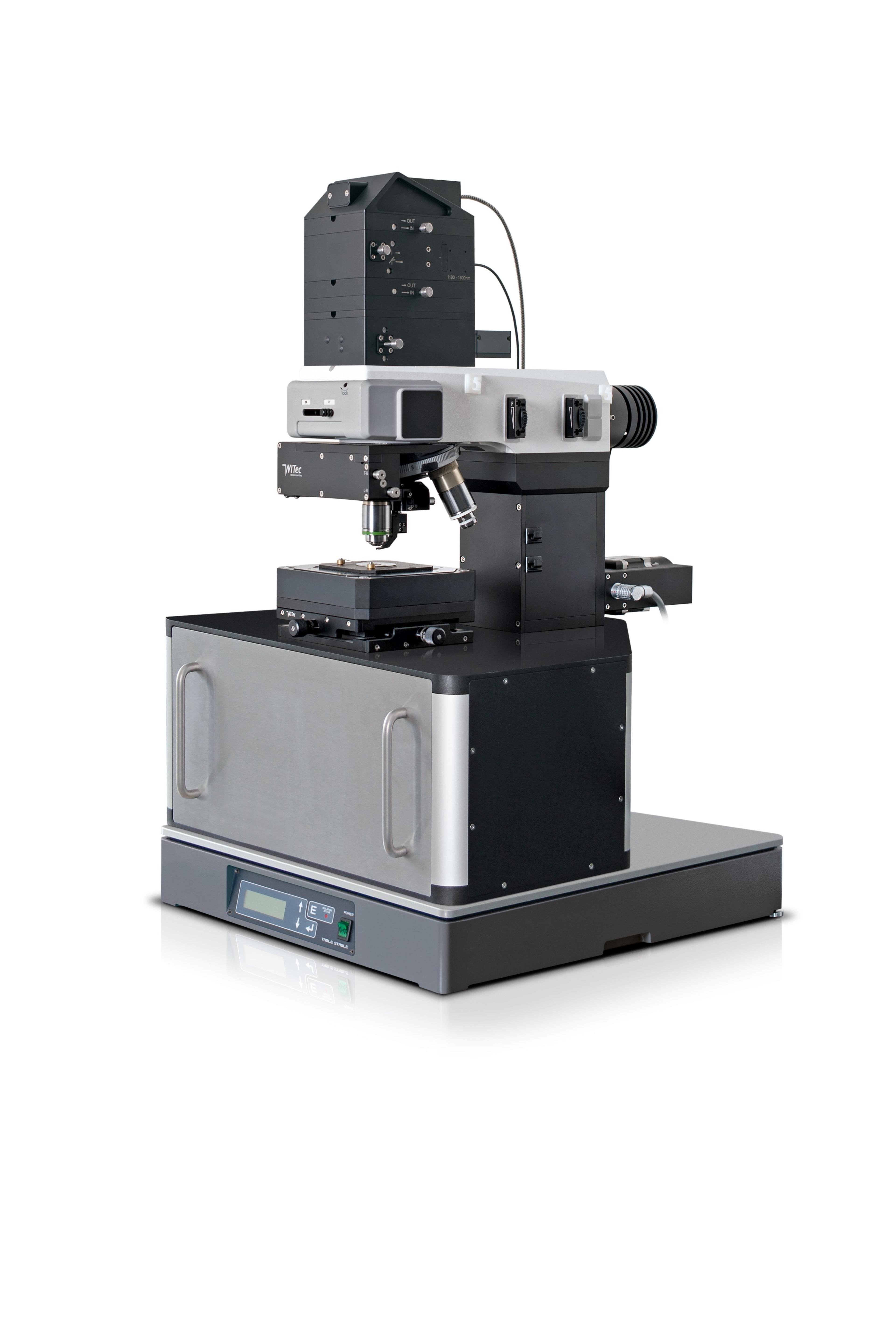
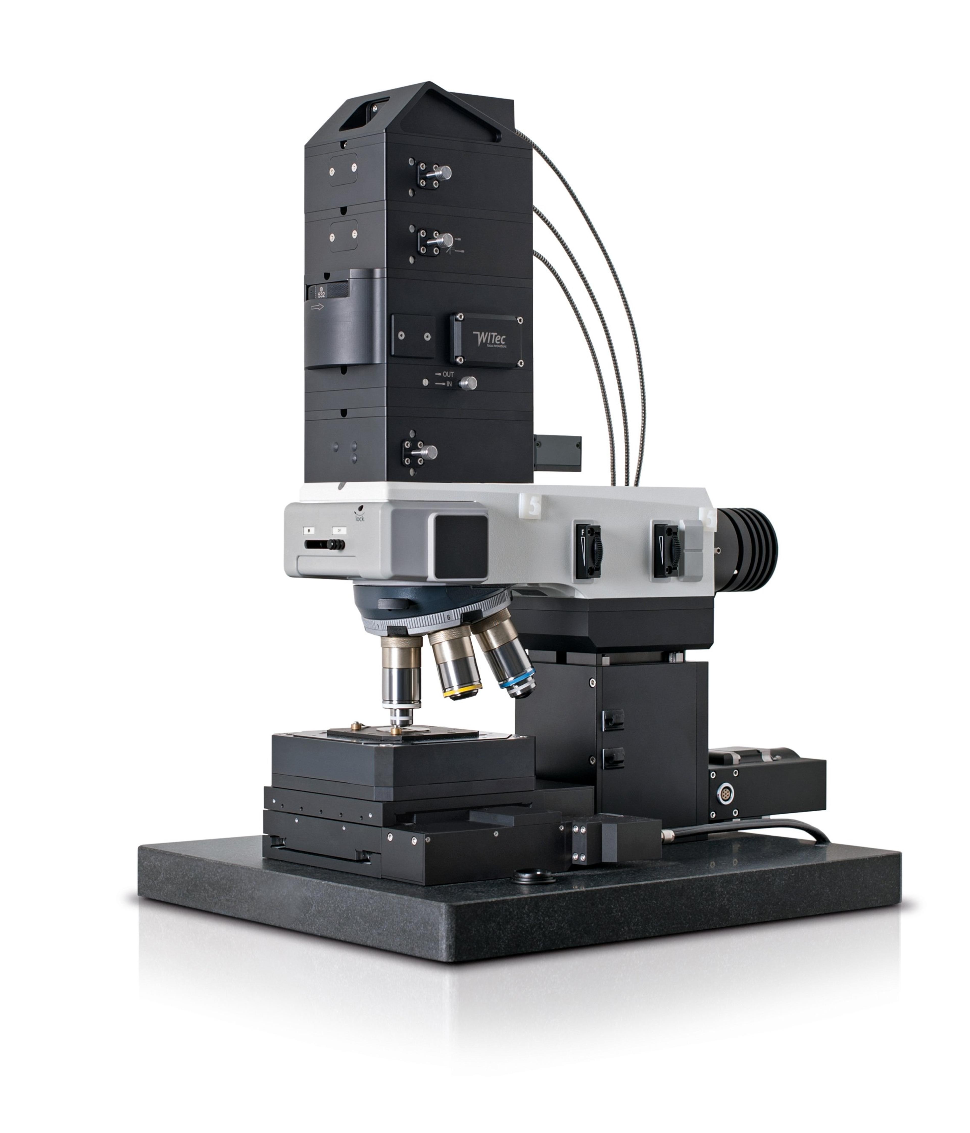
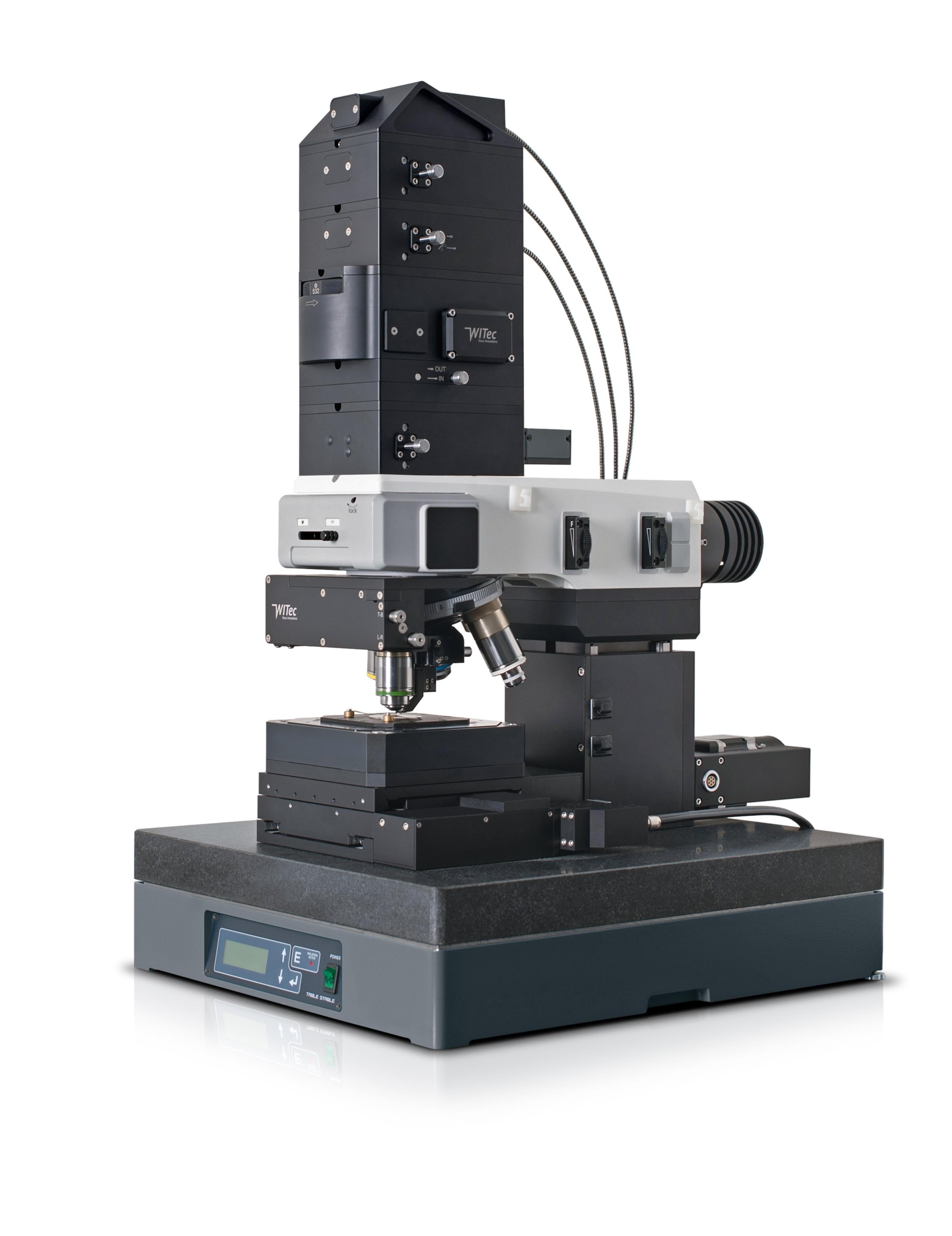
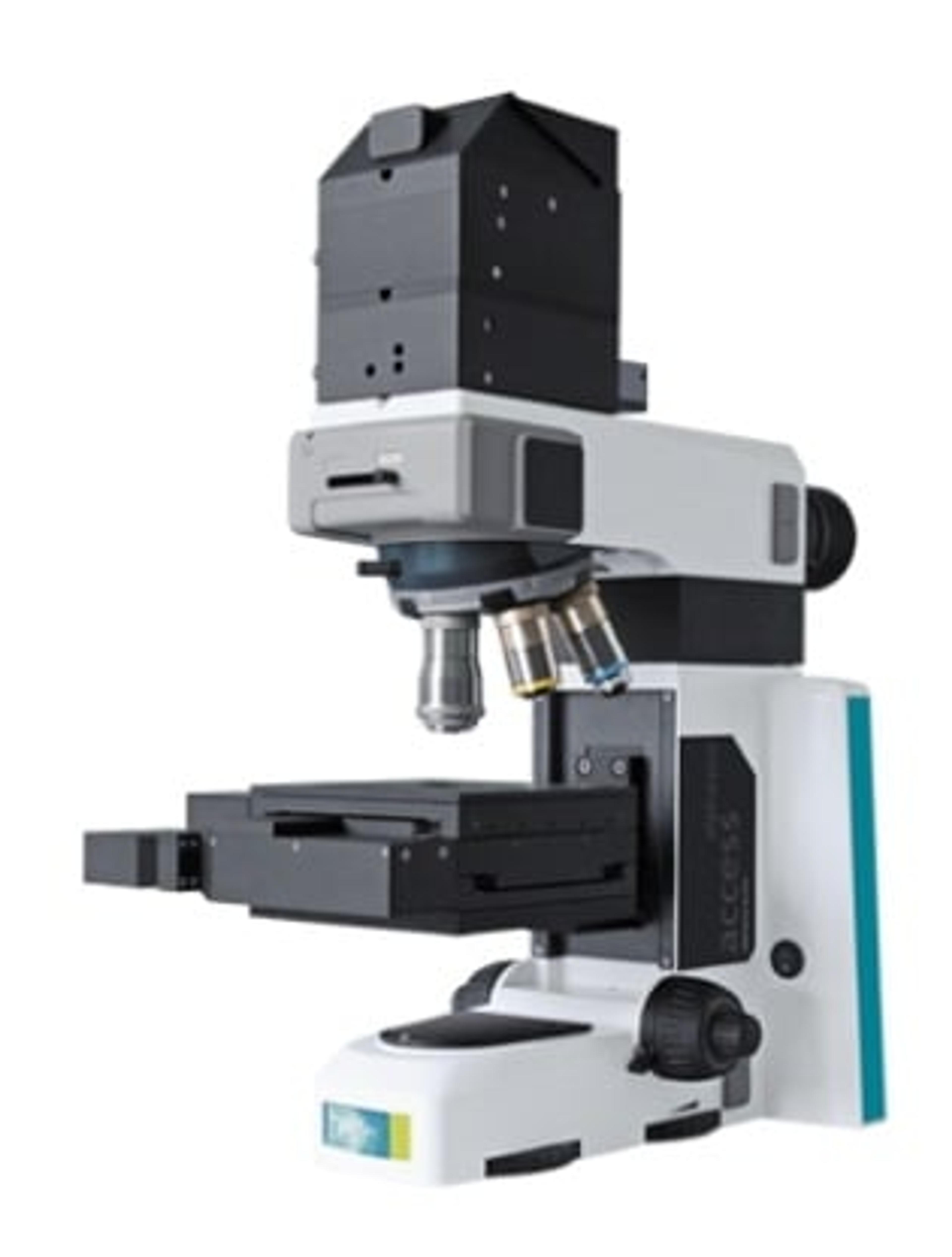
In the News – The Latest in Graphene & 2D Materials GRAPHENE SERVICE: New Partnership Seeks to Kickstart UK’s ‘Miracle Material’ Industry Industrialization of graphene has seen a step in the right direction with the National Physical Laboratory (NPL) and National Graphene Institute (NGI) at the University of Manchester UK teaming up to provide a leading standard characterization service of graphene for industry. Find out more here: New Graphene Service to Kick-start ‘Miracle Material’ Industry in UK >> GROWING 2D SHEETS: Bright Future for Flexible Electronics with Large Sheets of MoS2 2D material molybdenum disulphide (MoS2) has commercial application in photodevices and transparent sensors, but is limited by the difficulty of producing large uniform sheets. Researchers at the A*STAR Institute of Materials Research and Engineering have now developed a method to fabricate centimetre-sized monolayers of MoS2, which could also be applied to other 2D materials. Discover more here: Novel Applications for Remarkable 2D Material >> CRINKLED GRAPHENE: Regular Arrangement of Static Charge on Graphene Could be the Cause of Nanoscale Self-Assembly Regular self-assembly on the surface of graphene may lead to the development of advanced composite materials and technologies, coupling both materials' properties. Although it has been observed in the literature previously, a clear explanation as to why some molecules self-assemble on graphene’s surface has been lacking. A recent discovery made by researchers at Brown University could explain this phenomenon and provide a way to manipulate the self-assemblage of molecules on the surface of graphene. Find out more here: Electrically Charged Crinkles in Graphene Could Lead to Breakthroughs in Nanotechnology >> In the Lab – Application Notes and Methods TIP-ENHANCED OPTICAL SPECTROSCOPY: Revealing Nanoscale Variations in Optoelectronic Properties in MoS2 To engineer nanodevices integrating monolayer molybdenum disulfide (MoS2) — a promising 2D nanomaterial for next-generation photovoltaic solar cells, optoelectronic circuits and sensors — nanoscale opto-electronic characterization is needed. Learn how tip-enhanced optical spectroscopy (TEOS) enables characterization of opto-electronic properties on the nanoscale, such as the variation in emission within a submicron-sized flake, as well as information on the morphological, chemical and electronic structure. Learn more in this application note by HORIBA Scientific: Characterization of MoS2 Flakes using Tip-Enhanced Optical Spectroscopies (TEOS) >> DISCERNING LAYERS: In-situ SEM / Raman Study of Graphene Layers Although graphene is a monolayer, it can easily stack into two or more layers when preparing a sample or device, altering its properties. Therefore, it is important to accurately know if the sample is one-, two- or multi-layer graphene. Find out how the number of graphene layers can be easily attained and visualized in situ with this application note from ZEISS Microscopy: In-Situ SEM and Raman Investigations on Graphene >> CORRELATIVE RAMAN MICROSCOPY: A Comprehensive Analysis of 2D Materials Confocal Raman imaging is an ideal method for studying 2D materials, revealing their molecular characteristics through a non-destructive and fast procedure. Orientation of layers, defects, strain and functionalization can be revealed. Correlating this information with high-resolution microscopy methods gives a comprehensive analysis of your material in question. Discover how correlative Raman microscopy can help your 2D material investigation in this application note by WITec GmbH: Correlative Confocal Raman Microscopy for 2D Materials Investigation >> At Your Desk – Videos for Your Coffee Break NANO-RAMAN WEBINAR: Extensive Characterization of 2D Materials Properties Scanning probe microscopy is a fantastic nanoscale technique that can reveal a large amount of information on the physical characteristics of a material, however it lacks chemical sensitivity. In this webinar, Dr. Marc Chaigneau explores in depth the power of correlated AFM/Raman measurements for characterizing both the chemical and physical properties of 2D materials such as graphene, functionalized graphene oxide, MoS2, WS2 and MoSe2. Detailing the mechanism of tip-enhanced optical spectroscopy and how it can be effectively utilized to extract localized nano-properties of your sample. Watch the webinar here: NanoRaman Correlated Tip-Enhanced Optical Spectroscopy >> INTEGRATED ANALYSIS: Combination of High-Resolution SEM and Raman for Materials Analysis Raman spectroscopy can reveal information on the orientation, defects and functionalization of 2D materials, however, localized analysis is often required due to the nanoscale size of the sample. Find out in this video how the integration of ZEISS microscopy scanning electron microscopes with WITec’s Raman confocal imaging systems enables an effective high-resolution, and ease-of-use solution for materials analysis. Watch the video here: WITec ZEISS Partnership Enables Integrated SEM/Raman Workflow >> Receive more great content like this straight to your inbox, become a member for free today!