University Team Uses Deben's ARM2 Detector to Better Understand Catalytic Reaction Mechanisms
26 Jun 2018Deben, a leading provider of in-situ testing stages together with innovative accessories and components for electron microscopy, reported how the University of Tsukuba team of Professor Jun-Ichi Fujita have developed a method to visualize local fields at relatively low beam voltages using the Deben ARM2-STEM detector.
Jun-Ichi Fujita is a Professor in the Institute of Applied Physics at the University of Tsukuba and a member of the Tsukuba Research Centre for Interdisciplinary Materials Science (TIMS). He presented this work at the 61st International Conference on Electron, Ion and Photon Beam Technology & Nanofabrication, where he demonstrated high sensitivity visualization of localized electric fields using low energy electron beam deflection. This is of particular value to those working in the development of alkaline fuel cells for automobiles.
Professor Fujita describes his work: “The goal of our research project is to clarify the catalytic reaction mechanism and to improve the reaction efficiency for various applications such as fuel cell, dehydrogenation from methane, etc. The catalytic reaction realized on a nanoparticle should cause charge localization on a specific point. The localized charge creates a strong local field and such the strong electrostatic field could reduce the transition barrier of adsorbed molecules. Many researchers never doubted this reaction principle, but no one had ever demonstrated the real space imaging. We think our imaging technique contributes to the field of electrochemistry from our position as analytical physicists.”
Previous methods have employed electron holography in a transmission electron microscope but now Professor Fujita has demonstrated this performance using a low magnification scanning electron microscope, (Hitachi S-4800). This required instrument development, in particular, to improve the sensitivity of detection. This need led to collaboration with Deben and the use of their ARM2-STEM detector. Previously, Fujita's team had used conventional photomultiplier detectors with a gold grid line to measure the deflection angle of the primary electron beam. However, as the deflection angle is inversely proportional to the beam energy, their results were not clear. The ARM2-STEM detector overcame this.
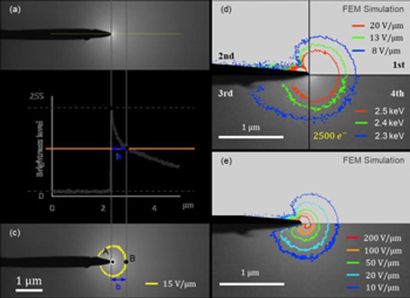
Part of the work is described here with the image from the paper published with the permission of the authors shown above. It shows the analysis method for the local field intensity. (a) Original STEM image, and (b) brightness profile along the yellow line in (a). The impact parameter b was defined by the position B having 50% of the brightness level (128). (c) Contour of the deflection shadow occupying 50% intensity of brightness. (d) Contour mapping of 20, 13, and 8 V/μm field intensities by superimposing the contours determined from different acceleration voltages of 2.5, 2.4, and 2.3 kV, respectively. Upper quadrant is FEM simulation. (e) Contour mapping of 200, 100, 50, 20, and 10 V/μm field intensities derived from a single STEM image and point charge model.
Do you use any Deben products or equipment in your lab? Write a review today for your chance to win a $400 Amazon voucher!