ZEISS Material Application Notes Available for Download
Find materials related application notes regarding ZEISS microscope systems
20 Dec 2016
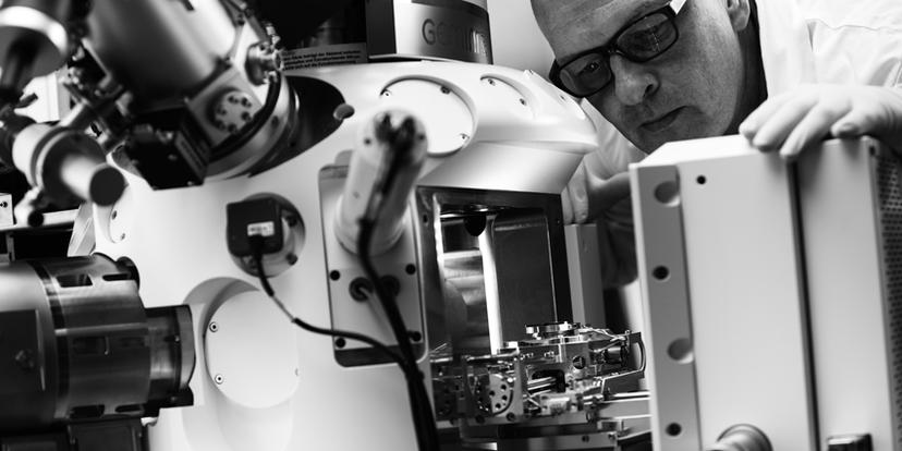
Image: Courtesy of ZEISS Microscopy
Carl Zeiss is a leading manufacturer of microscopes for the materials sciences. ZEISS systems are designed to provide you with the data you need, either for a fundamental understanding of materials, or to improve the composition of future materials. Comprehensive workflow solutions deliver multi-modal, multi-scale microscopy and analysis in 2D, 3D and 4D. This article comprises a selection of useful and interesting application notes from ZEISS microscopy, that are relevant to materials analysis.
1. Benefits of Low Voltage Back Scatter Imaging on ZEISS GeminiSEM Family
Traditionally, back scattered electron (BSE) imaging in scanning electron microscopes (SEM) is performed at relatively high beam energy (usually higher than 5 kV). On ZEISS GeminiSEM 300 / 500, low voltage BSEs can be effectively imaged by various methods with a landing energy down to 500 V. The two BSE imaging modes presented here enable the user to derive a wide range of information on material contrast or topography keeping resolution and contrast high at the same time.
2. Multi-Scale Correlative Study of Corrosion Evolution in a Magnesium Alloy
This application note describes the results of a multi-scale correlative tomography study on the corrosion of a Magnesium alloy. Zeiss’ Atlas 5 is used to efficiently link and navigate between in situ sub-micron X-ray microscopy, nanoscale X-ray microscopy and FIB-SEM tomography. The study provides a description of the complex crack and corrosion byproduct geometries which can lead to a more complete understanding of the underlying mechanisms for corrosion.
3. Microscopic Methods in Metallography Using ZEISS Axio Observer
Knowledge of the structure, crystal structure, and micromorphology, as well as elemental composition and distribution are essential for ensuring safety in designs and components of all sizes – ranging from fields of mechanical engineering and aeronautical engineering to power station engineering and electrical engineering. This application note demonstrates the high resolution analysis of metal samples using the ZEISS Axio Observer.
4. ZEISS Crossbeam - Enabling Smart FIB Work with SmartSEM
This application note describes SmartFIB, a new user interface for FIB operation in ZEISS Crossbeam instruments, and some of its capabilities. SmartFIB is an extension of SmartSEM, the operating software of ZEISS scanning electron microscopes, which is active for ZEISS FIB-SEM systems. SmartFIB allows the user to flexibly tailor his FIB milling strategy to obtain the desired results by providing access to all relevant parameters like dose, pixel spacing, pixel dwell time and FIB current.
5. ZEISS Xradia Ultra: Sample Preparation for Nanoscale 3D X-ray Microscopy
X-ray microscopy (XRM) enables 3D investigation of internal structure across a wide range of materials and length scales. The non-destructive nature of X-ray imaging uniquely enables in situ and 4D imaging, where the same sample is imaged multiple times under varying conditions to observe microstructural evolution. ZEISS Xradia Ultra offers non-destructive 3D imaging, bridging the gap between traditional micro CT or submicron resolution XRM. This application note introduces various sample preparation methods and tools that are available or can be adapted for use with Xradia Ultra.