ResourceSpectroscopy
High-Resolution 3D Confocal Raman Imaging for Group III Nitrides
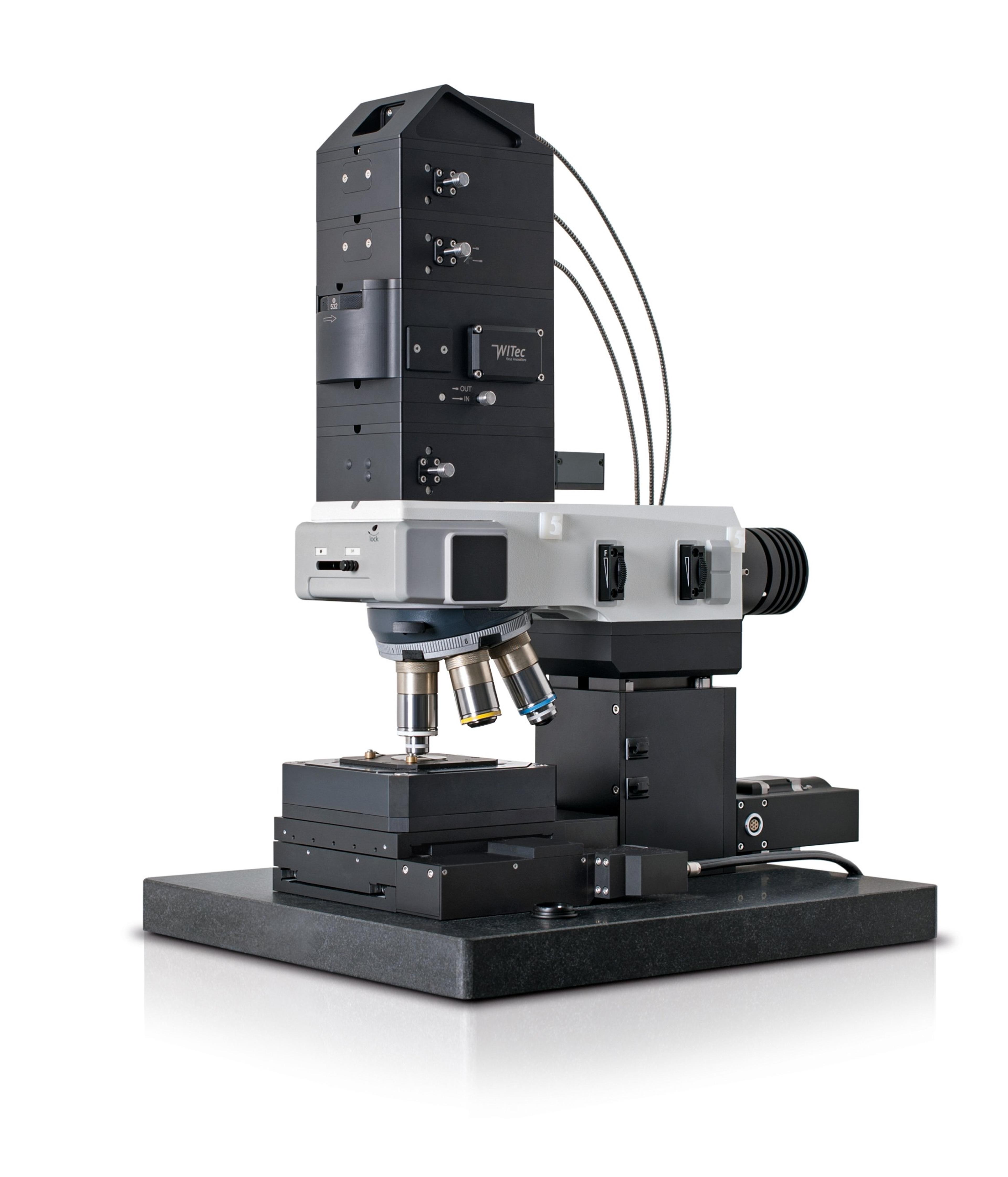
9 Nov 2012Structured substrates are widely employed in semiconductor research and especially in semiconductor development. The high demands on device quality and reliability make it increasingly important to have a detailed knowledge of the inherent strain and crystalline properties of device structures. X-ray diffraction and scanning electron microscopy are commonly employed for semiconductor characterization. In this application note from WITec 3D confocal Raman imaging was used to probe the properties of GaN layers grown on patterned substrates. Results are presented of the measurements that reveal changes in the signal which can be attributed to strain as well as changes in lattice structure.

