ResourceSpectroscopy
III-V Wafer Characterization through Photoluminescence Mapping
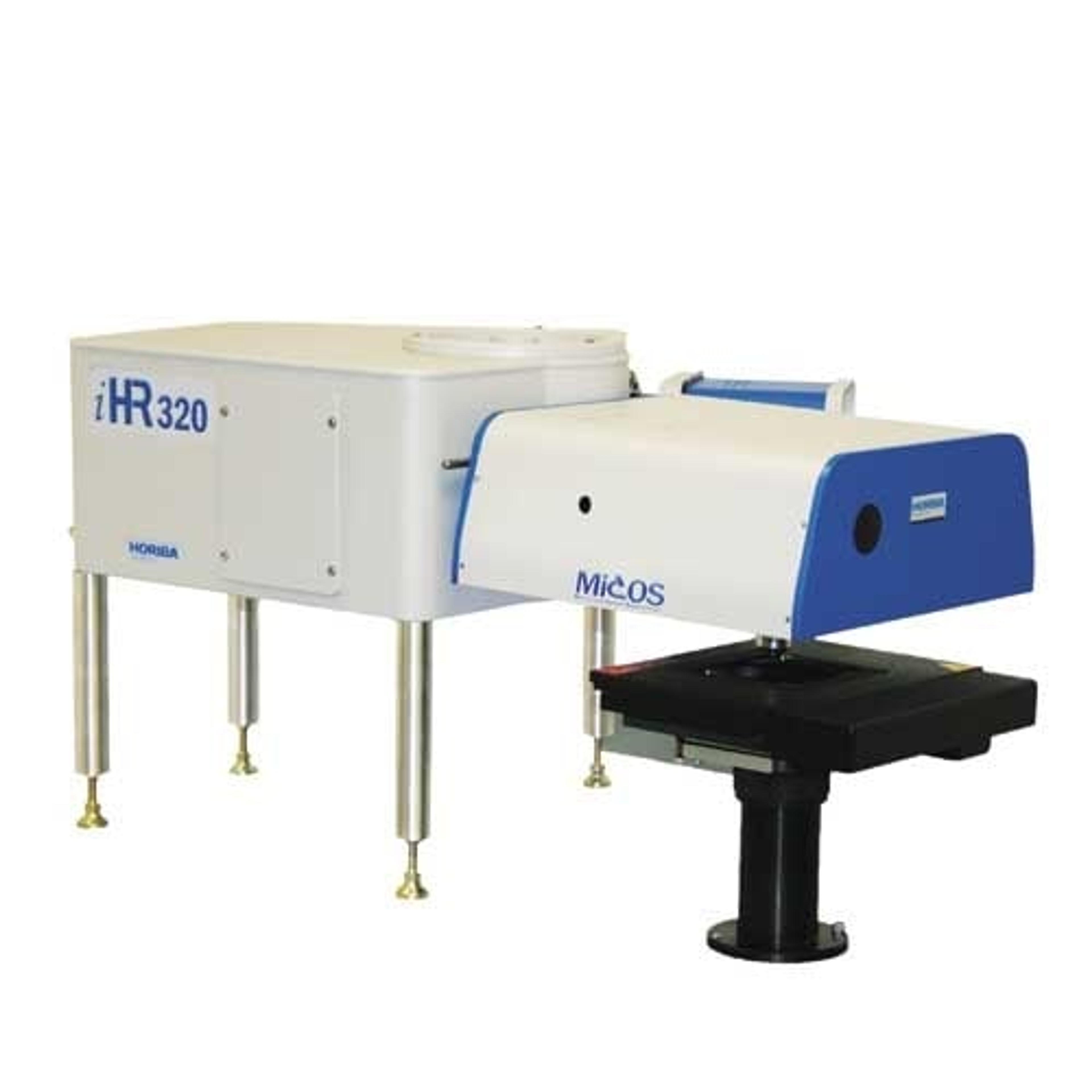
22 Dec 2017III-V semiconductors are important to the fabrication of active photonic devices such as light sources and detectors. Successful fabrication of such devices relies on the high quality of the underlying materials and precise deposition of intended geometries on a wafer substrate. Defective materials and imperfections in geometries adversely affect yield, and usually increase cost and development times. The cost and delay penalties are further compounded when such defects in either material or device-geometry are not caught early enough in the cycle.