How FT-IR spectroscopy is shaping the next generation of semiconductors
Learn how sophisticated FT-IR tools are advancing semiconductor research and manufacturing, from silicon purity testing to novel device characterization
8 Nov 2023
Four decades ago, the term "Silicon Valley" was coined to refer to the cluster of companies in California that pioneered the mass production of silicon-based semiconductors. Since then, the global semiconductor industry has experienced unprecedented growth, with silicon maintaining its position as the most dominant material in semiconductor manufacturing.
To ensure high semiconductor efficiency and performance, quality control in the form of the identification and quantification of impurities, detection of defects, and functionality testing of optical devices has become a crucial task. To this end, FT-IR spectroscopy has emerged as a powerful tool to investigate the fundamentals of semiconductors in a highly sensitive, fast, and non-destructive manner.
In this article, SelectScience® speaks with Dr. Michael Jörger, Head of Business Unit Science at Bruker Optics, to learn more about the role of FT-IR spectroscopy in the analysis of semiconductor materials and how instruments from Bruker can effectively support industries and research communities from material development and manufacturing quality control to final device characterization.
Looking beyond silicon
Silicon-based semiconductors underpin practically everything we take for granted in our digital world: from smartphones and laptops to solar panels, cars, and airplanes. However, as semiconductor technology continues to advance, requirements for silicon purity and manufacturing accuracy are becoming increasingly demanding. At the same time, many researchers are seeking new semiconductor materials that could offer even greater processing speeds and efficiency.
While Jörger is in no doubt that silicon will continue to dominate the semiconductor market, he notes that new materials are emerging for certain applications and market segments, such as in the field of optoelectronics. Optoelectronic devices integrate photonics and electronics into a single semiconductor-based device capable of generating, detecting, and manipulating light. They have a broad range of applications from solar cell technology to dedicated optical sensors, LED or laser-based devices and even medical applications.
“Many exciting innovations are occurring in this field, including the development of new types of optical sensors and the use of new types of light sources,” Jörger enthuses. “These devices are typically not based on just one bulk semiconductor material but instead use so-called heterostructures, made up of several layers of semiconductor material in periodical structures such as quantum wells, super lattices, or quantum dots.”
Another area where alternative materials to silicon are being researched is for power semiconductor devices, which form a critical component of power management systems used in large-scale applications such as railways, industrial inverters, and renewable energy distribution. “Traditionally, these were based on silicon, but are being replaced more and more by wide gap semiconductors, such as silicon carbide and gallium nitride,” says Jörger. “These offer advantages over silicon in terms of performance, efficiency, and reliability, and are sooner or later expected to completely replace silicon-based power semiconductor devices.”
The role of FT-IR spectroscopy
For semiconductor material research and development, FT-IR spectroscopy stands out as an easy and effective tool for the investigation of several fundamental material parameters. “FT-IR spectroscopy can be used to determine critical parameters such as the bandgap, lattice vibrations, layer thickness, and doping concentration,” says Jörger. Additionally, this technique can also be employed to characterize the final optoelectronic devices. “For instance, if someone has developed a novel type of light source, FT-IR can be used to determine the spectrum with very high spectral resolution, but also with time resolution. If someone develops or produces optical sensors, we can also adapt these to our spectrometers. In other words, we can use the customer sensors as detectors and then determine the detection characteristics of that sensor.”
In the development and production of power semiconductor devices, FT-IR spectroscopy is equally useful for determining parameters such as layer thickness and doping concentrations can serve as a crucial quality control measure. “These analytics pay into the final device quality, and so are extremely important,” asserts Jörger.
While FT-IR is being increasingly used in the development of new semiconductor materials, Jörger notes its primary application in the industry is for detecting elemental impurities and defects in silicon during semiconductor manufacturing. Here, the sensitivity of FT-IR instruments is essential, as “the lower the impurity concentration is, the better prices silicon suppliers can get on the market,” he says. Ease of use is also key, as users are typically not spectroscopists. “Many of them prefer push button operation or at least a well-defined workflow with robust data analysis and convenient reporting of the relevant result parameters,” he says. “Wherever possible, they also prefer to have measurement and evaluation procedures which are linked to official standards like ASTM or SEMI.”
Dedicated FT-IR tools for semiconductor research and manufacturing
As a leading supplier of spectrometry instruments, Bruker Optics offers a comprehensive portfolio of benchtop and at-line FT-IR spectrometers designed to meet critical semiconductor analysis needs across a broad range of applications, from R&D to process improvement. As a result, a significant fraction of the world's top semiconductor manufacturers rely on Bruker metrology tools. “These include dedicated and customized solutions such as the Cryogenic Silicon Analysis System (CryoSAS), an all-in-one silicon analyzer dedicated for industrial environments,” shares Jörger. “The CryoSAS system allows users to obtain all relevant impurity concentrations, including carbon and oxygen, as well as "shallow impurities" such as boron, phosphorus, and others. This fully automated instrument is the first of its kind and sets the industry standard for the quality control of solar grade or electronic grade silicon according to ASTM/SEMI requirements.”
In addition to detecting impurities down to a low ppta range, the CryoSAS operates without the need for cryogenic liquids, reducing both safety risks and running costs. “Bruker now has several different solutions to achieve sample cooling without the need to handle unhandy and often expensive cryogenics such as liquid nitrogen or liquid helium,” explains Jörger. “These include techniques such as closed-cycle cooling, pulse tube cooling, or stirling cooling.”
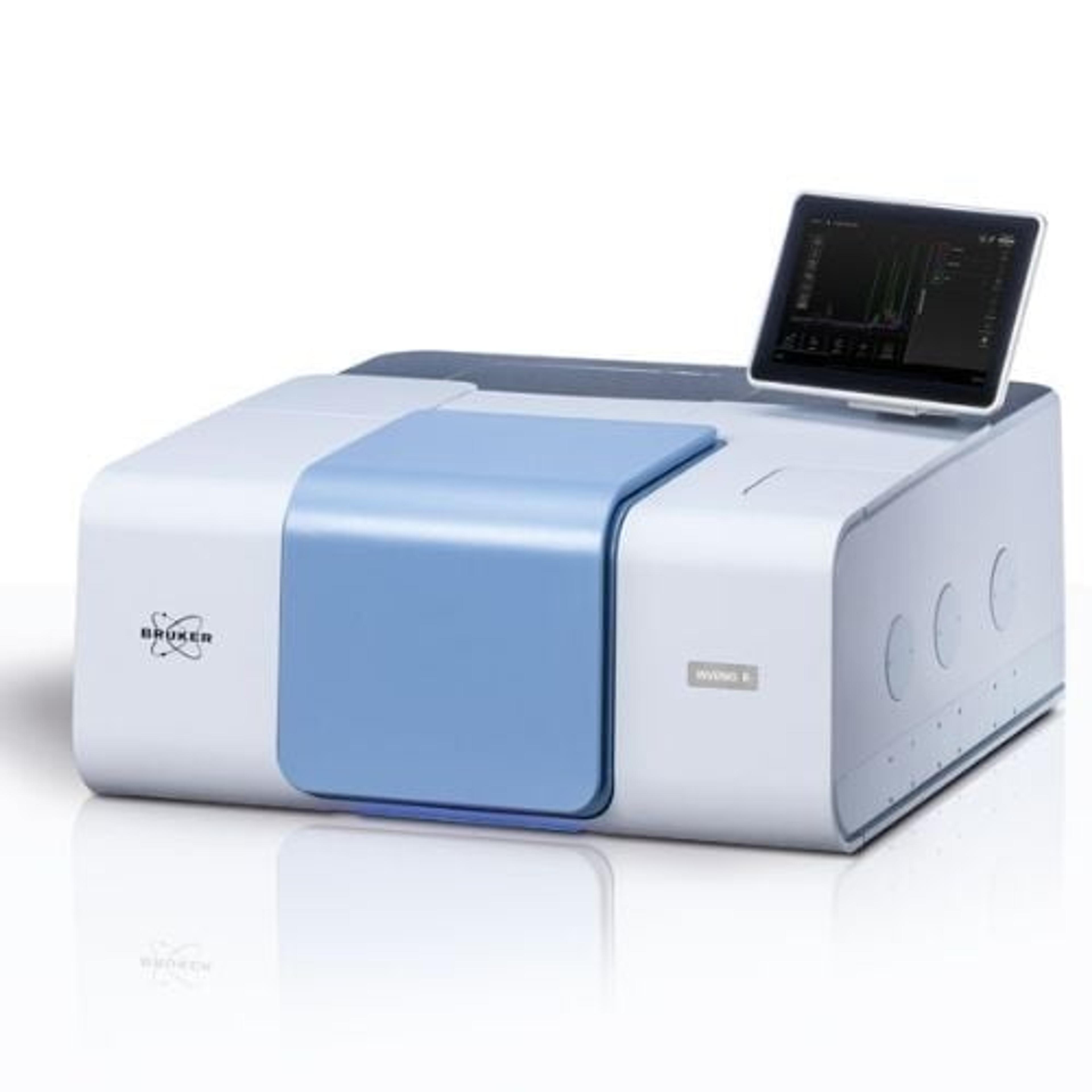
For analytical and research applications, Bruker offers the bench-top VERTEX and INVENIO series, designed to combine greater versatility with unmatched sensitivity. The VERTEX series, including the entry-level VERTEX 70v and high-end VERTEX 80/80v features a vacuum optics bench that completely eliminates atmospheric absorption artifacts such as water vapor, resulting in improved sensitivity and stability. “INVENIO, on the other hand, is a highly modular and easy to use platform: an analytical toolbox, which can exactly be tailored to customer requirements from very different fields” shares Jörger.
INVENIO is built upon Bruker’s highly precise and robust interferometer technology—and is compatible with a broad range of accessories and external modules. The system can be extended from FIR to VIS/UV spectroscopy, time-resolved spectroscopy, and simultaneous MIR/FIR measurement. It is also available with an automated 3-position beam splitter changer and an additional sample channel. “Users can really tailor it exactly to their requirements,” he adds.
While Bruker is well-known for the high specifications of its instruments, Jörger emphasizes that there have also been notable advancements in its software over the past decade. “When I started at Bruker over 18 years ago, there was uniform software for every customer,” he says. “Now, we have optimized software workflows with customization and touch operation, and we can even design customer-specific workflows. These start with early feasibility tests and progress to developing customized numerical evaluation models, and even Python-based user interfaces.”
Industry trends
Looking to the future, Jörger is particularly excited to see how the semiconductor industry will contribute to the green energy transition, not only in photovoltaics but also in power semiconductors. He also highlights the continued development of optoelectronics devices, such as the use of vertical-cavity surface-emitting lasers (VCSELs) in facial recognition technology for smartphones, as well as their potential in other applications.
Lastly, he acknowledges the trend towards deglobalization in the semiconductor market, with major companies like Intel investing in new production sites in different regions. “For several decades, almost everything was produced in Asia, but this will change now for several reasons,” he says. “This means the semiconductor industry will be much more geographically diverse, and possibly there will also be more players than before.”
“As an instrument manufacturer, we're excited about this development and look forward to supporting these companies on their journey,” he concludes.