Innovating Energy Storage Materials using Correlative Microscopy
SelectScience® spoke to Professor Silke Christiansen, Freie Universität Berlin, and Helmholtz Center for Materials and Energy, about a new era of microscopy
18 Apr 2016

SelectScience® spoke to Professor Silke Christiansen, Freie Universität Berlin and Helmholtz Center for Materials and Energy, about a new era of microscopy
Helmholtz-Zentrum Berlin for Materials and Energy (HZB) The HZB explores materials and complex material systems that help to face current and future challenges. One of the HZB’s research emphases is on materials for thin-film photovoltaics and for the conversion of solar energy into chemical energy carriers (e.g. molecular hydrogen).
By training a materials scientist, Professor Silke Christiansen, Freie Universität Berlin, leads an institute at the Helmholtz Center for Materials and Energy where her team studies everything “from semiconductors to other materials with specific electrical and optical properties”. The uniting factor is that “everything is at the nanoscale”. She recently presented at the European Molecular Biology Laboratory conference ‘From 3D Light to 3D Electron Microscopy’, organized in conjunction with ZEISS Microscopy.
At the Helmholtz Center, her team is working on “new sorts of solar cells and fuel devices”, she explained, developing complex nanomaterials to “convert solar energy into other forms of energy, such as heat or chemical energy”. “There are many, many challenges, the biggest of which is storage”, she revealed. There has been a huge rise in the production and use of renewable energy but “all these new forms of renewable energy have to be stored to be used throughout times when they cannot be produced”.
All nanoshapes and sizes
“Very often, we use nano wires, because they have a huge aspect ratio – a small diameter and a long length – so they have a large surface that can be functionalized”, Prof. Christiansen explained. Her team uses “all sorts of molecules” to tune the surfaces of the nanowires, “such as those that terminate the surface, additional layers that can absorb solar light and materials that can guide electrons to electrodes”. For solar storage, materials need to “be a semiconductor and need to have the right bandgap to absorb the solar energy, which is most efficient in the green part of the spectrum”, said Prof. Christiansen, so “semiconductors like silicon of different shapes and sizes, or III/V materials such as gallium nitride or gallium arsenide” are used.
The power of microscopy
Working with nanoscale, microscopy is crucial to visualize “what materials we have, and where the objects are”. For a solar cell, different properties need to be optimized, “so we need correlative microscopy, where what we see is correlated to optical and electrical measurements”. From artificial and natural materials to medical and biological samples, “we need correlative microscopy to optimize and advance understanding of future materials”.
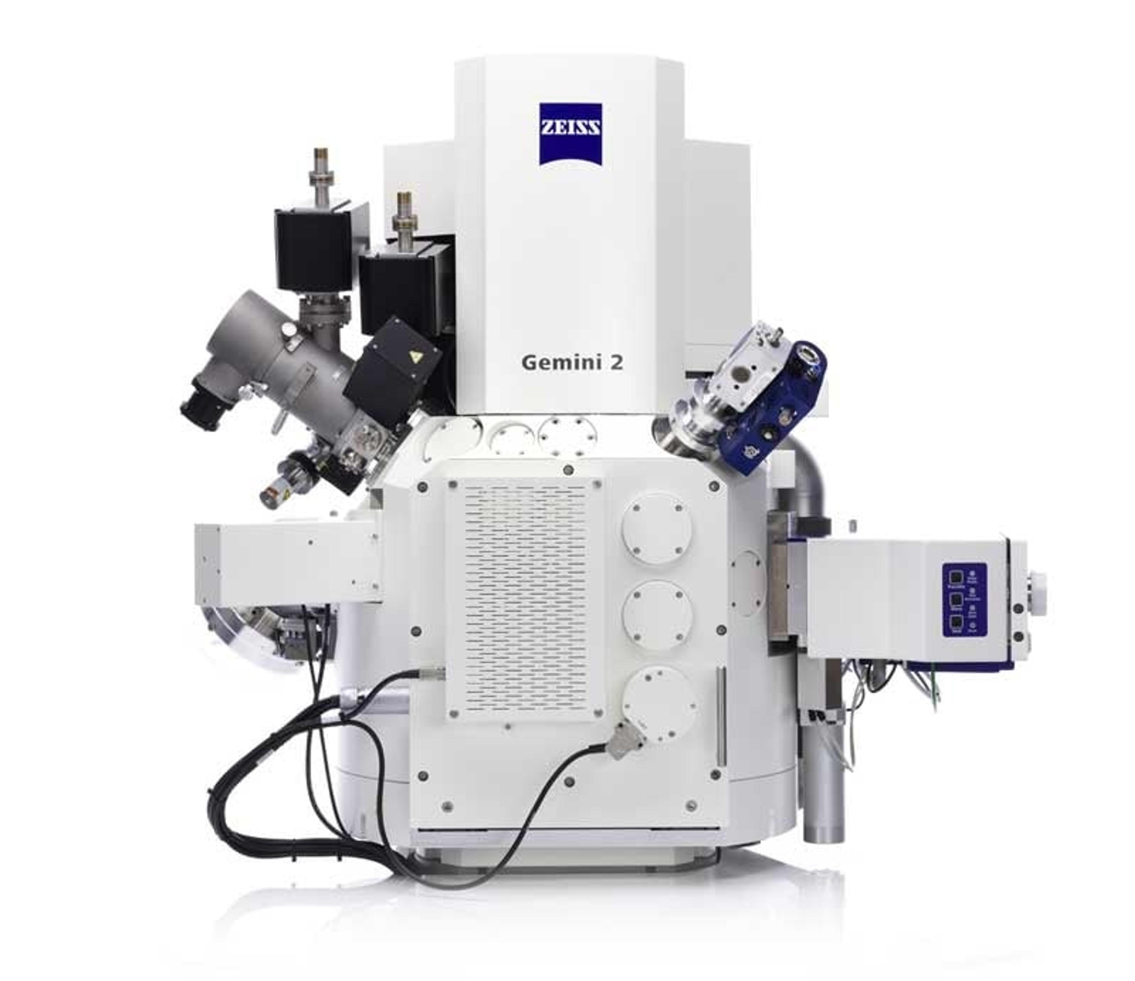
This ongoing and cutting edge research has been made possible through “very unique equipment from ZEISS”, Prof Christiansen revealed, such as the scanning electron microscopes (SEM) MERLIN and ORION. Correlative microscopy “brings many techniques together”, and ZEISS have developed a “smarter” door system where “different doors with different functionalities” can be used, or removed. Therefore, she explained, “instead of having multiple techniques crammed together, you can use only the technique you want to use for that sample”.
“We have come to a new era of electron microscopy”, explained Prof Christiansen. “We can ask and answer questions we could never answer before”. The technique is being applied to real world samples, such as bone and tissue in a collaboration with the medical department of Prof. Dr. Georg Schett at the University of Erlangen, looking at bone structure in osteoporosis. However, the possibilities are endless: “today, we don’t even know what there may be available in the future”.

