Editorial ArticleMaterials
Pixel-level tuning of Timepix4 advances detector technology
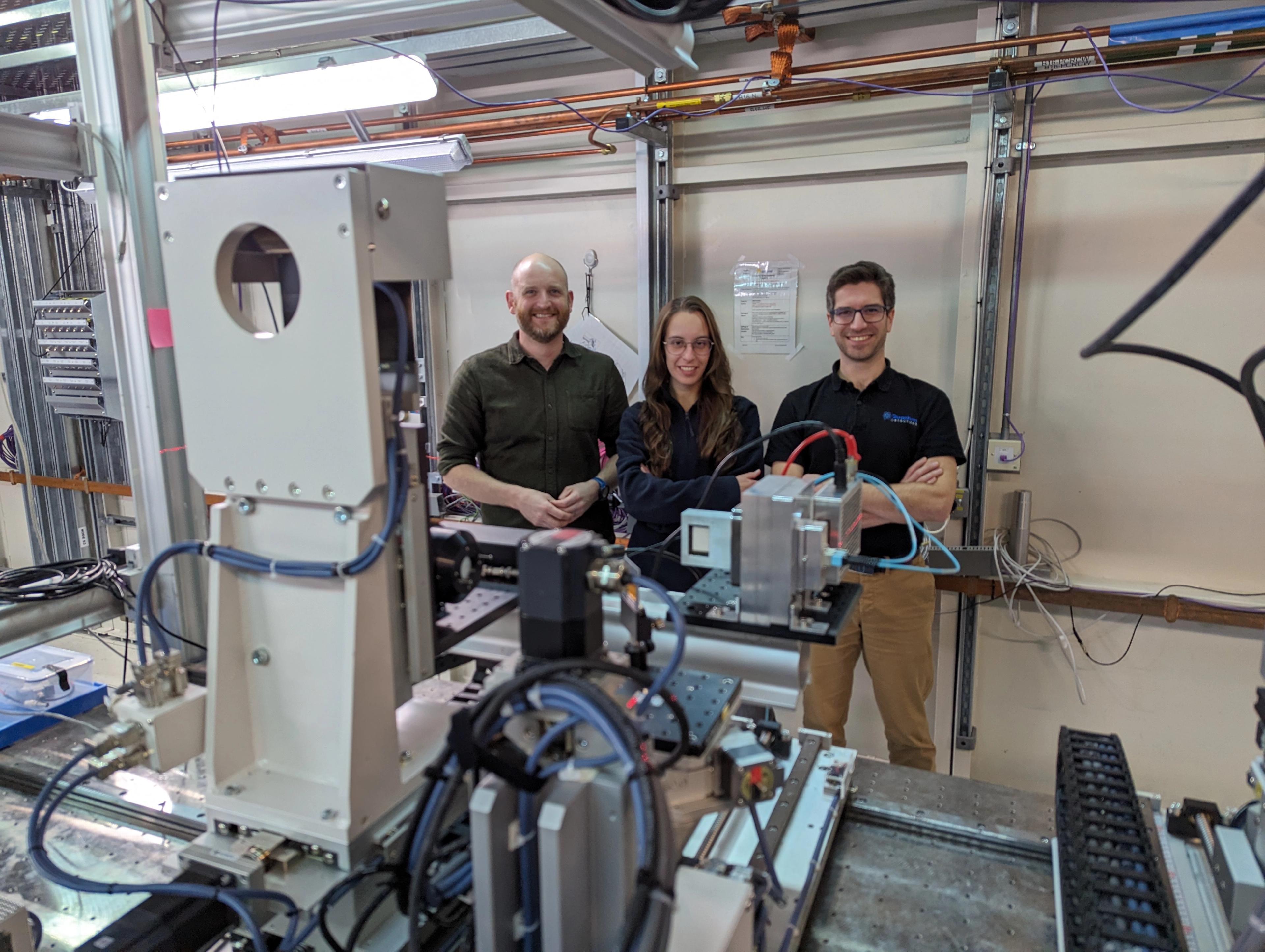
Oxford researcher Nina Dimova pushes pixel-by-pixel calibration and clustering to unlock nanosecond precision in particle tracking and electron microscopy
Scanning Electron Microscopy (SEM) is a technique that uses a focused electron beam to scan a sample and create high-resolution images. It is widely used in materials science, nanotechnology, and biological research. Explore SEM systems in our peer-reviewed product directory; compare products, check reviews, and get pricing directly from manufacturers.
Oxford researcher Nina Dimova pushes pixel-by-pixel calibration and clustering to unlock nanosecond precision in particle tracking and electron microscopy