Level up your high-resolution imaging: Demonstrating the Phenom Pharos G2 FEG-SEM
Watch this on-demand webinar to discover how the Phenom Pharos G2 FEG-SEM can progress your nanomaterial research
20 Oct 2022

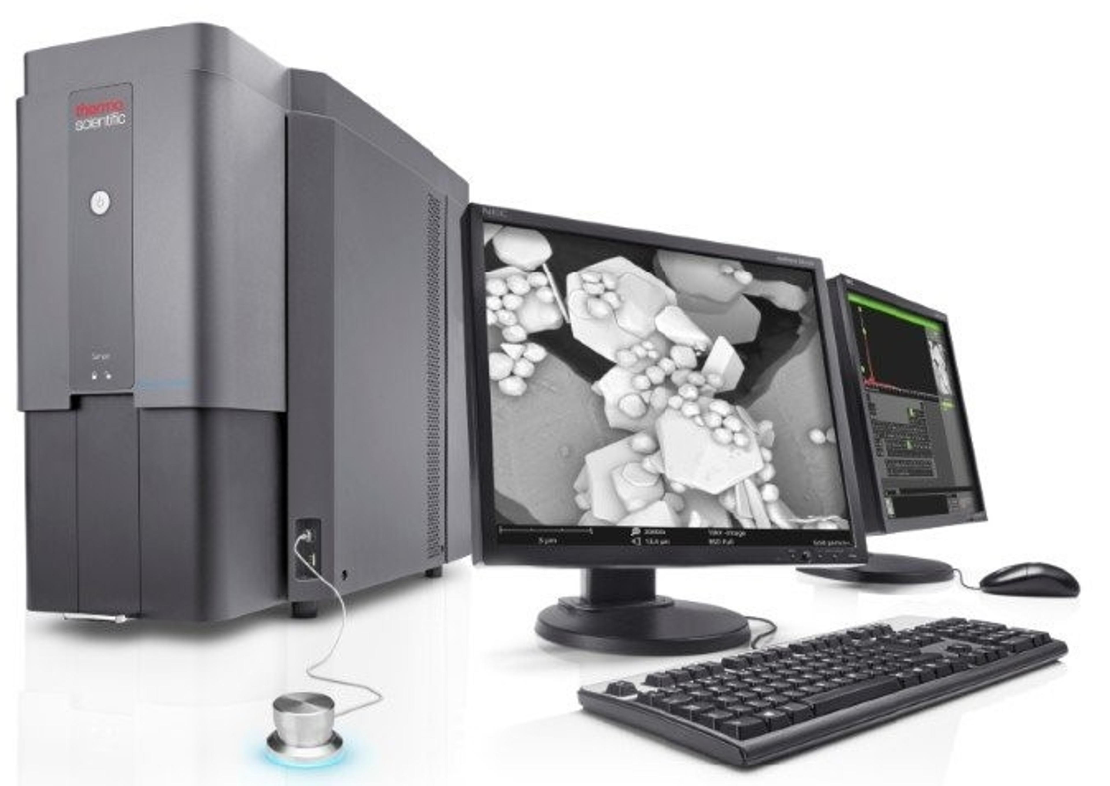
Nanotechnology research redefines how we live, and field emission gun scanning electron microscopy (FEG-SEM) has revolutionized nanoparticle research. The Thermo Scientific™ Phenom™ Pharos G2 Desktop FEG-SEM progresses nanomaterial research by delivering high resolutions and a wide acceleration voltage range, all in a desktop system that can fit within a lab or office.
In this SelectScience webinar, now available on demand, Keriya Mam, product and application SEM engineer, Thermo Fisher Scientific, demonstrates how the Phenom Pharos G2 Desktop FEG-SEM is intuitive to operate and highly productive, making it a versatile instrument for high-volume industrial and academic labs.
Watch on demandThink you’d benefit, but missed the live event? Register now to watch the webinar at a time that suits you or read on for highlights from the Q&A session.
Please can you comment on which samples require coating, why you used platinum, and when you can don’t need coating?
KM: If I'm dealing with a conductive specimen or a hard material, for example, a rock, mineral, or ceramic, I would not use any coating. Specimens which typically need coating include sub-material like polymer or biospecimens like tissue.
I will always try to coat the specimen with platinum. The main reason why is the Phenom Pharos G2 FEG-SEM will distinguish the grain coating from gold and platinum. I tend to not use gold as with the gold coating, we introduce a lot of artifacts from the coating, which are less visible with the platinum. Platinum is also the most suitable coating for higher resolution.
Does the software include an optical profilometry feature? If so, what beam do you recommend?
KM: We have an application, which is called 3D R-R and this is capable of taking multiple images using a basket electronic detector and rebuilding these images together to get 3D information on your specimen. The 3D R-R is available from all the Phenom desktop SEM.
Is there a limit to the kV you can use for studying polymer ceramics or metallic samples?
KM: No, all kVs can be used. You can always start from a high kV for conductive specimens to do your analytical work, and then lower the kV to see if you can see contamination or dust. There are things at low kV which you may not see at high kV.
How does the Pharos compare to other types of SEM that don’t have a field emission source?
KM: It depends on the application. If it's for low mag, then I would say they're both equal. But if you're dealing with smaller structures where you must go to higher mag and higher sensitivity, then FEG is needed.
Please can you talk a little bit about automation on the Pharos?
KM: The first application I can think of is called automated image mapping. This feature acquires a series of images in X and Y and stitches the images together like the Google maps principle. It is standard on all Phenom desktop SEM.
We also have a dedicated team working on the Phenom Programming Interface (PPI), and this helps the operator to make a method for them to be able to drive the stage to a different position or to acquire data at a different modification. With thanks to PPI, we can develop some fully automated solutions for some applications.
What is the smallest detail that the Pharos can see?
KM: If you really push the system to its limit, and the sample is super friendly under the beam, you can measure 10-nanometer feature size. It's not something you're going to look at every day. If you want to look at a 10-nanometer particle, 2 or 0-nanometer particle, every single day, then maybe Pharos is not the solution for you. But otherwise, from 20 nanometer onwards, we can easily see the particle or the feature size.
What is the best way to deal with charges on the image?
KM: It's nice when you have a specimen which is charge-free, but you can have a sample which can be full of charge. Charge obscures the features you want to see but by going to lower kV, it can just disappear because the signal from the sample and the primary beam can cancel each other out. The best way to deal with charges is simply by lowering the voltage, lowering current and increasing the pressure or coating the specimen.
Want to learn more about the Phenom Pharos G2 FEG-SEM, watch the full webinar here>>
SelectScience runs 10+ webinars a month across various scientific topics, discover more of our upcoming webinars>>