Sustainable nanotechnology innovations fuel nanomaterial synthesis for electronics, photocatalysis, and energy
Dr. Daniela Gomes shares her work on metal oxide nanostructures and reveals how advanced microscopes from ZEISS have transformed the quality and impact of her group's research
8 Oct 2023

Harnessing the unique chemical and physical properties of nanomaterials is one of the most promising scientific pursuits of the twenty-first century. From ultra-efficient solar cells and lightweight batteries to innovations in environmental remediation, sensing, and biomedicine, nanomaterials have the potential to deliver major benefits to society and the planet.
Dr. Daniela Gomes is an Assistant Professor at the CENIMAT/i3N research center of the NOVA School of Science, University of Lisbon, Portugal. Her research is focused on the production and structural characterization of metal oxide nanomaterials, primarily for sensor and photocatalysis applications.
We spoke with Dr. Gomes to learn more about her research and how she is working toward the sustainable synthesis of metal oxide nanomaterials. Dr. Gomes also shares some of the emerging challenges in the field of nanotechnology and highlights the crucial role played by advanced microscopy tools in guiding nanomaterial synthesis and device optimization.
Greener synthesis of metal oxides
Metal oxides are a versatile class of materials that display many favorable properties, including enhanced electrical and optical characteristics, high optical transparency, chemical stability, and in some cases biocompatibility. When the size of metal oxide materials is reduced to the nanoscale level, high surface-to-volume ratios and surface reaction activities offer further benefits, making them attractive for applications ranging from energy conversion and storage to electronic devices, self-cleaning surfaces, and photocatalysis.
Given their vast potential, the sustainable production of metal oxide nanomaterials is highly desirable and forms a core focus of Dr. Gomes’ research. “Our goal is to produce these materials in as green a way as possible,” she explains. “This involves utilizing low-cost abundant materials, employing low-temperature methods, and using water-based solvents and environmentally friendly substrates."
Several chemical and physical methods have been reported for the synthesis of metal oxide nanomaterials, including sol–gel, atomic layer deposition, electrospinning, anodization, and sputtering. However, these methods typically require high temperatures and/or long reaction times, making them energy intensive. For this reason, Dr. Gomes and her team are focusing on hydrothermal/solvothermal synthesis routes assisted by microwave irradiation. “Microwave heating is a simple, fast, and energy-efficient alternative to conventional methods,” she illustrates. “While conventional heating in ovens can take hours and requires high temperatures, microwave synthesis can be completed within minutes at temperatures around 100°C.”
Microwave irradiation not only minimizes energy consumption but also enables precise control over synthesis parameters, offers uniform and selective heating, and can lead to increased reaction yields in shorter timeframes. Moreover, it is compatible with flexible substrates like paper, which can further reduce the environmental footprint of fabricated devices. “We aim to use substrates such as paper, cork, and nanocellulose, as these are earth-abundant, lightweight, biodegradable, and can be recycled or repurposed,” Dr. Gomes states. “Similarly, we’re trying to use solvents that are more eco-friendly, such as water, and avoid reaction precursors that are dangerous and harmful to the environment.”
Dr. Gomes and her team have already published several pioneering studies employing these synthesis techniques for titanium dioxide (TiO2) and zinc oxide (ZnO) nanomaterials, including for photocatalysts on cork and paper,[1–3] paper-based electrochromic devices,[4] and UV sensor applications.[5]
Emerging challenges
While titanium dioxide and zinc oxide have been incorporated into various products, such as sunscreen, and are generally regarded as safe and green materials, Dr. Gomes recognizes the potential unintended risks associated with nanomaterials on both the environment and society. “Ensuring safety is a significant challenge with all nanotechnology, and when working with increasingly smaller nanomaterials, material recovery becomes crucial,” she says. “We still don’t know the effect of many nanomaterials on the environment and human health, and trying to understand their long-term behavior and toxicity is a major priority in the field.”
Balancing the performance and environmental impact of nanomaterials also remains a critical challenge. “We know some materials work better when made using certain precursors or solutions that are not ideal from an environmental perspective,” she adds. “It is imperative that we continue to seek ways to reach the same level of performance using greener options.”
The right tools for the job
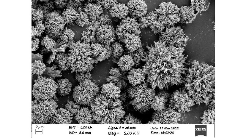
As is often the case in nanotechnology research, multi-physical characterization tools play a pivotal role in Dr. Gomes’ work. “We always start with scanning electron microscopy (SEM), to try to understand if we achieved what we were hoping to during the synthesis,” she says. “Following this, we employ a multitude of characterization techniques, including scanning transmission electron microscopy (STEM), Raman spectroscopy, UV-Visible spectroscopy, X-ray energy dispersive spectrometry (XRD) as well as other techniques to determine electrical properties for particular applications.”
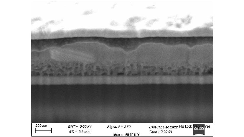
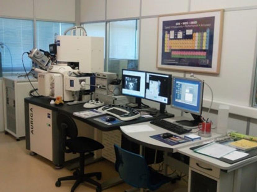
To this end, Dr. Gomes and her team rely heavily on microscopes and detectors from ZEISS, including the AURIGA FIB-SEM workstation for surface and cross-section SEM observations. “The AURIGA microscope was the first SEM microscope installed at CENIMAT and marked a turning point in the growth of our group,” Dr. Gomes shares. “Even today, ten years later, it continues to be a core support of our research activities and is the only focused ion beam (FIB) microscope on campus.”
The AURIGA is a predecessor to the ZEISS Crossbeam family, a suite of modular instruments that combine the powerful imaging and analytical performance of Gemini electron optics with a next-generation FIB for material processing and sample preparation.
These FIB-SEM instruments enable high-resolution morphological, structural, and elemental analysis of nanostructured samples in both 2D and 3D, while also facilitating precise milling and deposition for the manipulation and fabrication of nanodevices. “In our research, the FIB-SEM is critical for performing cross-sectional internal characterization and failure analyses, and we also use the AURIGA for TEM lamella preparation for STEM,” shares Dr. Gomes. “We also have several additional detectors on the instrument, including EDS for elemental analysis, EBSD for crystallographic analysis, as well as characterization tools for collecting electrical measurements.”
In addition to the performance and usability of its microscopes, Dr. Gomes is also quick to praise the team at ZEISS, who she says has played a pivotal role in supporting her group’s research. “Even though ZEISS is a huge company, they listen to everyone, and they have really helped us elevate the level of our research,” she says.
“In Portugal, we work directly with ZEISS engineers from Spain, and for more delicate applications, we also enlist help from the branch in Germany, who reply almost instantly,” she adds. “If we ever needed to buy another FIB, it would be from ZEISS.”
The future of nanomaterial characterization
Looking ahead, Dr. Gomes envisages the techniques and technologies underpinning nanomaterial characterization progressing in two main areas. The first is a growing trend towards correlative microscopy, whereby multiple imaging modalities, length scales, and dimensions are integrated to gain comprehensive and complementary information about nanoscale structures and their properties. “We have to understand how materials behave on both a nano and macro scale to get the full picture,” she explains. “ZEISS is way ahead on this. For example, we’re using a ZEISS confocal microscope in conjunction with the AURIGA, performing fluorescence microscopy before investigating an area of interest using FIB-SEM.” ZEISS Atlas 5 software can help in this regard, as it enables images from SEM, FIB-SEM, X-ray, and light microscopes to be quickly and efficiently correlated and analyzed.
The second area, perhaps unsurprisingly, is the increasing integration of artificial intelligence. “Each time we use any characterization technique, we generate a huge amount of data,” Dr. Gomes explains. “Being able to correlate this data, for example the electrical behavior of a sample to its optical behavior, is an area where AI looks to be very promising.”
“But it needs to be accurate, and as we know from the recent processing tools driven by AI – this isn’t always the case,” she adds. “These algorithms will need careful development to generate reliable results and help researchers better understand their structural, optical, and electrical measurements. This is evolving fast, but we’re not quite there yet,” she concludes.
References:
1. Nunes, D., et al.., 2021. Metal Oxide-Based Photocatalytic Paper: A Green Alternative for Environmental Remediation. Catalysts, 11(4), p.504.
2. Matias, M.L., et al., 2022. Floating TiO2-Cork Nano-Photocatalysts for Water Purification Using Sunlight. Sustainability, 14(15), p.9645.
3. Ferreira, S.H et al., 2021. High UV and Sunlight Photocatalytic Performance of Porous ZnO Nanostructures Synthesized by a Facile and Fast Microwave Hydrothermal Method. Materials, 14(9), p.2385.
4. Nunes, D., et al., 2020. TiO2 Nanostructured Films for Electrochromic Paper Based-Devices. Applied Sciences, 10(4), p.1200.
5. Pimentel, A., et al., 2017. Ultra-Fast Microwave Synthesis of ZnO Nanorods on Cellulose Substrates for UV Sensor Applications. Materials, 10(11), p.1308.