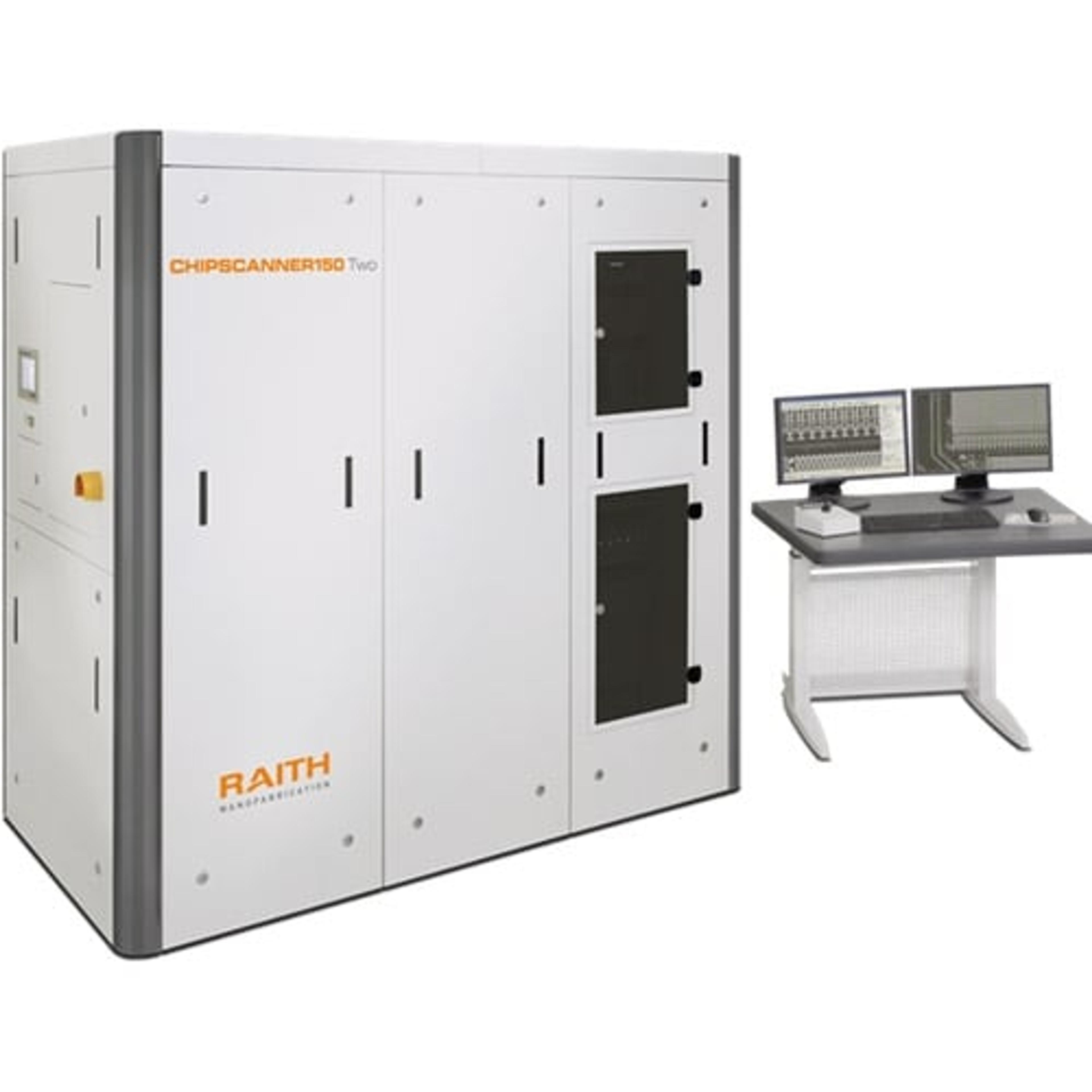
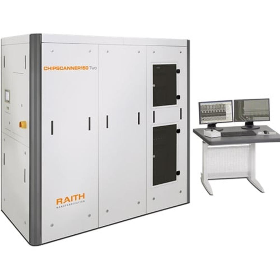
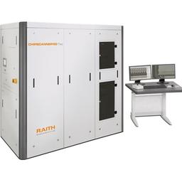
CHIPSCANNER
Large area image acquisition

The supplier does not provide quotations for this product through SelectScience. You can search for similar products in our Product Directory.
An amazing electron microscope!
Electron microscopy
The RAITH CHIPSCANNER with its environmental enclosure and its laser interferometer stage allows unique and unmatched accuracy on imaging large areas without any drift problems.
Review Date: 24 Dec 2020 | Raith Nanofabrication
3D SEM image mosaics stitched over large areas and in 3D with CAD shape extraction
The CHIPSCANNER combines high-resolution electron optics, multiple high-efficiency electron detectors, and ultra-precise Laser Interferometer Stage technology with unique software to deliver homogenous large-area image mosaics for each layer with minimum stitching errors and stable brightness/contrast values and CAD shape extraction. Features include:
- Active focus control using laser height sensing
- Highest position and beam accuracy and stability
- A wide range of selectable electron detectors
The CHIPSCANNER produces the most accurate large-area, high-resolution image mosaics directly acquired by an SEM instrument. Since the absolute position of each pixel, even over cm², is ultimately known to the accuracy provided by the laser interferometer stage and ultra-precise image calibrations, these images can be precisely stacked (3D-stitched).
Various high-speed detectors, flexible working distance, parallel detector stream handling and a high-speed scan generator allow precise and flexible image acquisition that is also high throughput.
Large-area, ultra-high-resolution 3D SEM imaging applications in chip reverse engineering, materials science, and life sciences (e.g. connectomics) require surfaces of up to cm² areas to be scanned with nm resolution and excellent layer to layer accuracy (‘3D stitching’) for layout and schematic extraction or 3D modeling. While traditional SEM instruments are inherently limited by small, uncalibrated fields of view (FOVs) and imprecise sample positioning, the CHIPSCANNER addresses these challenges by combining the resolution and flexibility of an SEM instrument with the accuracy, stability, and automation of an electron beam lithography (EBL) instrument – a core area of expertise at Raith. High-resolution, large-area image mosaics are created by capturing sequential SEM images and stitching them together for further analysis, while the laser interferometer stage and field-of-view calibration reduce overlap to an absolute minimum and thus reduce required computing. A true large-area 3D SEM!