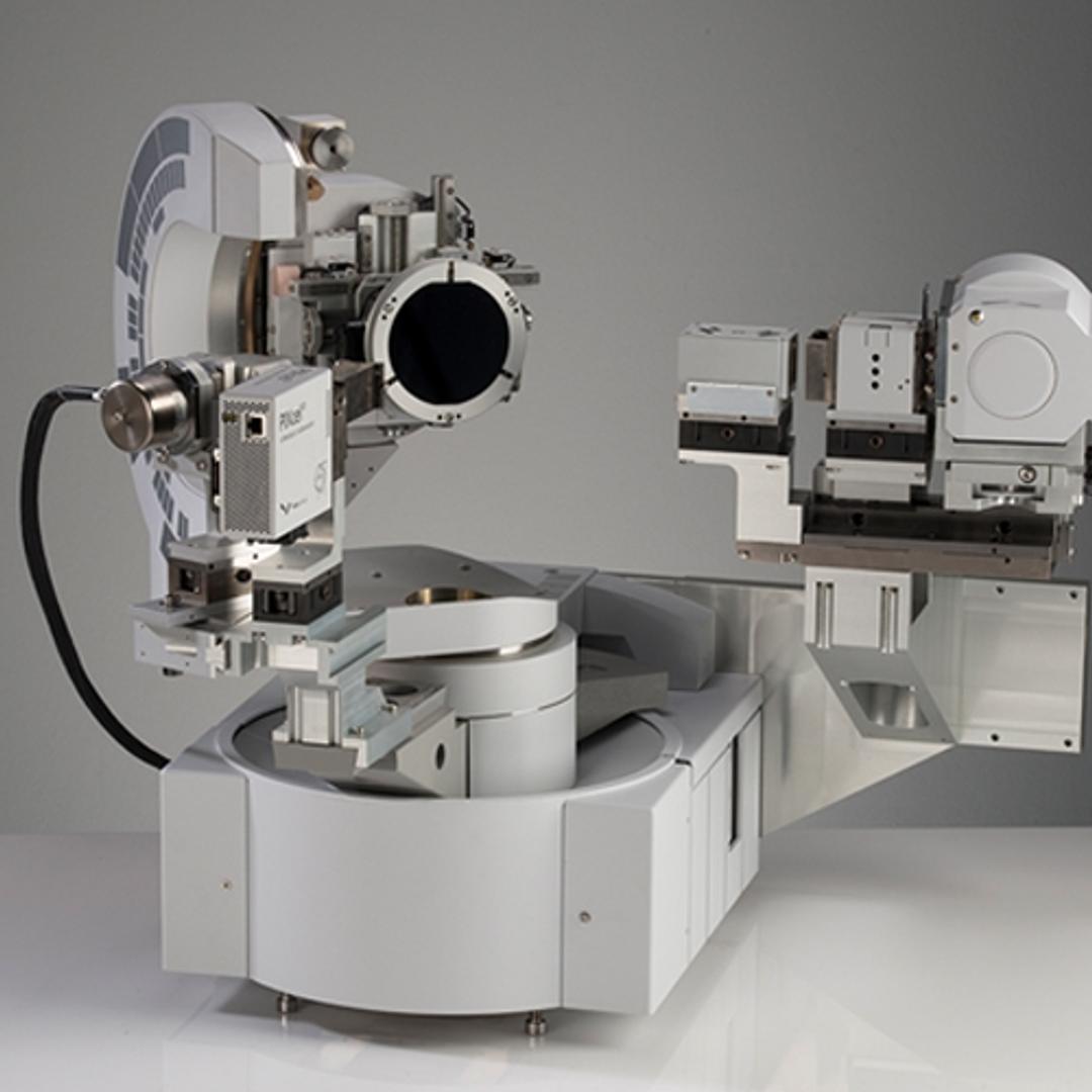
X'Pert3 MRD - XRD
Versatile research & development XRD system
High resolution XRD is one of the cost-effective, fast, and non-destructive methods for analyzing thin film materials
Wide bandgap semiconductor thin film, ohmic contact metal films, LD
On the one hand, using this device can easily measure the crystallinity and grain size of polycrystalline thin films, and can test superconducting thin films, ohmic contact metal films, etc. On the other hand, XRR function can be used to accurately measure the thickness of ultra-thin films, nanomaterials, and amorphous layers (ranging from 5-200nm), which is one of the economically applicable, fast, and non-destructive solutions. In addition, high-resolution XRD can also be used to measure the structural layer quality, thickness, stress, and alloy composition of GaN, GaAs ,InP and other series of thin film materials to promote the research and development process.
Review Date: 19 Nov 2024 | Malvern Panalytical
It is very necessary to use XRD for phase identification of any compound
Crystallographic information
It gives information on phases, structures, favored crystal orientations (texture), and different structural parameters, such as strain, crystallinity, medium grain size, and crystal cracks.X-ray diffraction analysis (XRD) is a method used in materials science to determine the material’s crystallographic structure.
Review Date: 6 Sept 2022 | Malvern Panalytical
Provides great results and can't imagine any material research without this.
Analysis of stress, strain, dislocation development in thin film during deposition under different g
We got a High-resolution XRD instrument, and the facilities provided are helping us to characterize epitaxial and amorphous thin films, pellets, and single crystals up to a resolution of 0.0001°. It also provides XRR and RSM facilities along with depth profiling. The software provided is pretty much user-friendly and the analysis obtained is vast enough. Whenever we got any issues we directly contact the engineer and without excuses, he reaches us for help. It's been 13 years of the machine but still provides reliable results which could be reproduced if conditions are maintained the same for example z, omega, etc.
Review Date: 6 Sept 2022 | Malvern Panalytical
Good result
Various area of fields, like a cement, polymers, Metals, ceramics, pharma
Instrument as well as good to work, advance function system is useful for getting good results.
Review Date: 16 Dec 2021 | Malvern Panalytical
User friendly instrument
Pharmaceutical, materials and nanomaterials
In our instrumentation facility PXRD instrument play a important role. we are getting good results and more than 50 research articles published in a good impact factor journals.
Review Date: 15 Dec 2021 | Malvern Panalytical
I recommend this seller.
Analyzing crystallite phase
We achieved high quality results, durable, and easy to use. The manufacturer provide a good warranty and excellent after sales services. They provide advice and maintenance and fast replies of communications.
Review Date: 14 Dec 2021 | Malvern Panalytical
Great results and this instrument is a boon to our research
Crystal studies
We achieve high quality reproducible results.
Review Date: 15 Nov 2021 | Malvern Panalytical
Great instrument, very versatile
Mineralogical identification
Easy to use, no need for gas or other supply. If it was developed to contain a database, it would be great.
Review Date: 18 Sept 2021 | Malvern Panalytical
Beyond expectations
Materials characterization
It is important in science to be stay updated about available resources or services to characterize the materials more efficiently.
Review Date: 17 Sept 2021 | Malvern Panalytical
Manufacturer's Response
Thanks a lot for taking the time to review our instrument. We are glad you are satisfied with it, in particular with our aftersales. We wish you many years of cutting edge research with it.
Results are very fine and useful for the researcher.
Structural study
Malvern Pananytical instruments are useful and results are good. The instruments are user friendly so new researcher can easily operate. Provided softwares are give the more calculations and new measurements. Further gives more accurate results for the scientific purpose.
Review Date: 13 Aug 2021 | Malvern Panalytical
The long and successful history of Malvern Panalytical's Materials Research Diffractometers (MRD) continues with a new generation – X’Pert³ MRD and X’Pert³ MRD XL. The improved performance and reliability of the new platform have added more analytical capability and power for X-ray scattering studies in:
- Advanced materials science
- Scientific and industrial thin film technology
- Metrological characterization in semiconductor process development
Both systems handle the same wide range of applications with full wafer mapping up to 100 mm (X’Pert³ MRD) or 200 mm (X’Pert³ MRD XL).

