ResourceMaterials
In-situ mechanical testing of semiconductor devices
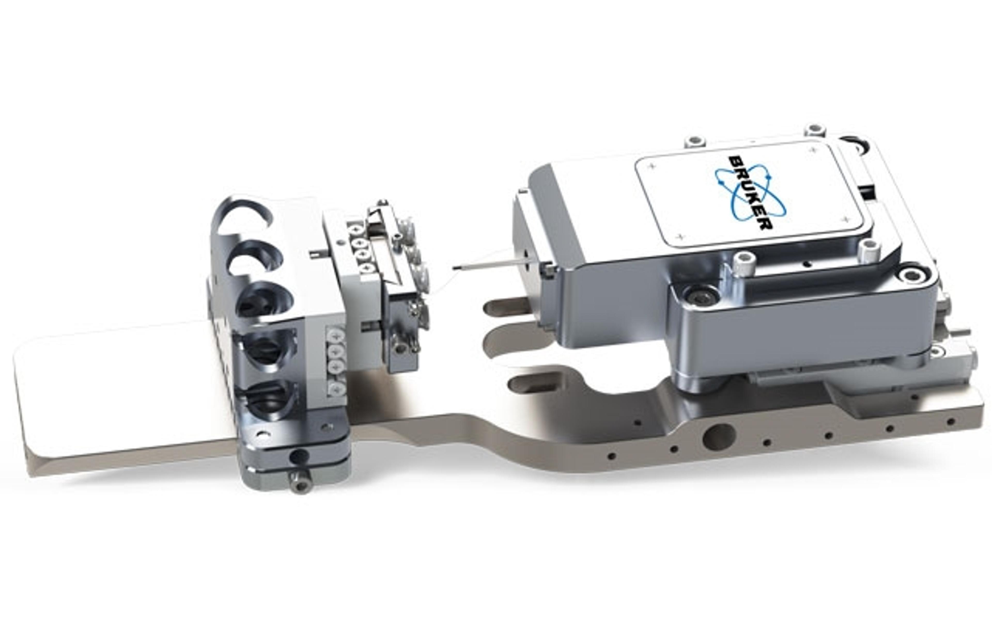
6 Jul 2023As advancements are made in the performance of semiconductor devices, changes in materials and processing techniques are often required. The trend towards miniaturizing these devices inherently involves components at or approaching the nanoscale. The mechanical properties of materials at this scale can be vastly different from bulk material, which introduces new concerns both during processing and in field use. A reliable testing technique is critical for evaluating the structural stability of these devices. In this application note, Bruker Nano discusses the use of the Hysitron® PI 85L SEM PicoIndenter® for the investigation of the failure mechanisms involved in FIB-milled back-end-of-line (BEOL) microbeam samples.