ResourceMaterials
SEM and EDS analysis in industry
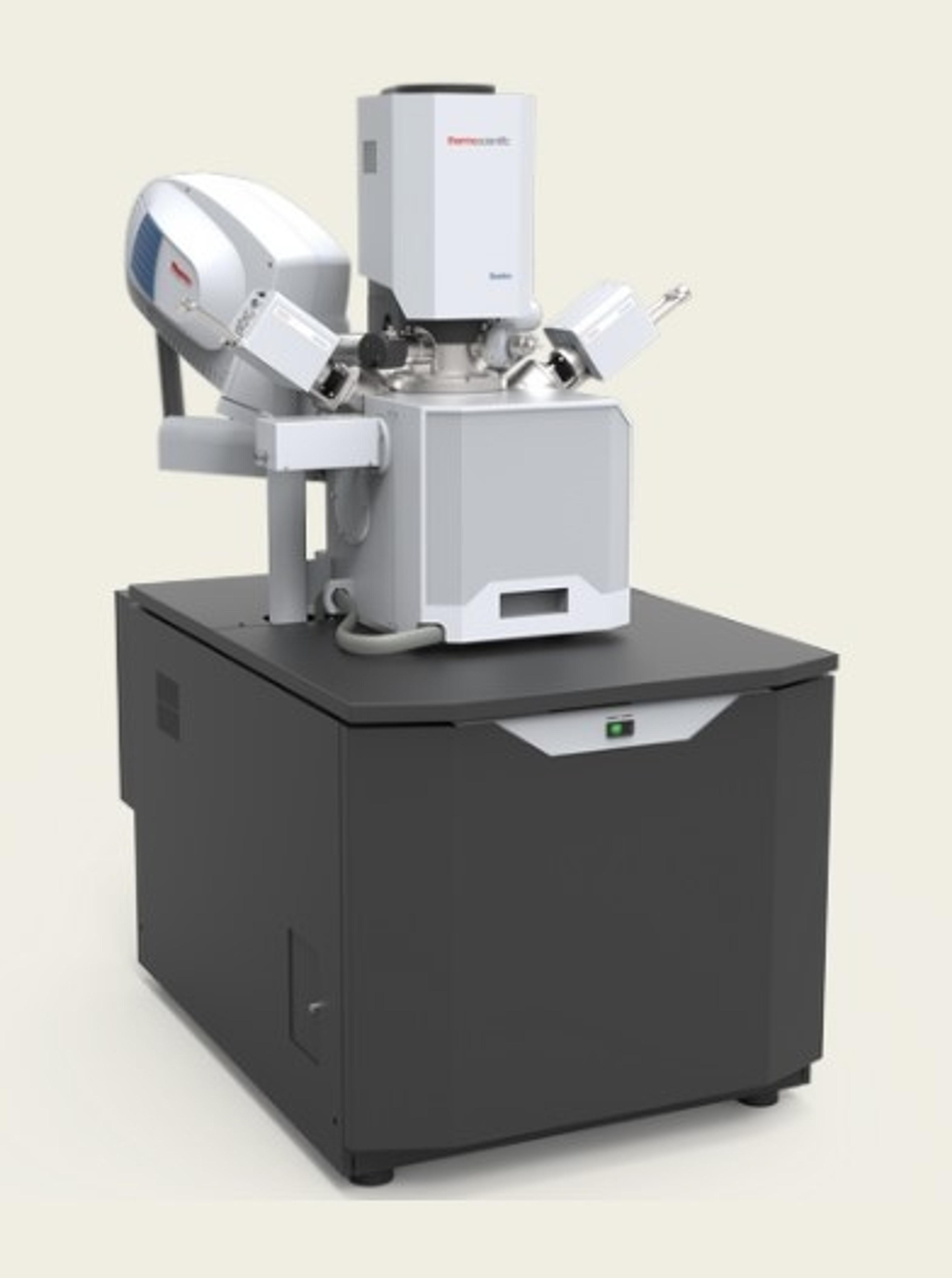
19 Feb 2021As the complexity of industrial processes increases, so does the need for more rigorous, high-quality analysis to ensure that products meet all standards of quality and reliability. Scanning electron microscopy (SEM) has become a common tool for modern research and development, as well as for failure analysis and troubleshooting, because it provides detailed (nanometer-scale) information about the surface structure of samples. SEM is often used in conjunction with energy dispersive X-ray spectroscopy (EDS), which adds elemental information to the surface imaging data.
Download this ebook to learn more about:
- How the joint application of SEM and EDS analysis supports in-depth material characterization for industrial applications
- How Thermo Scientific ColorSEM Technology is designed to integrate these two techniques into a single, fast, easy-to-use package, accessible to novices and experts alike


