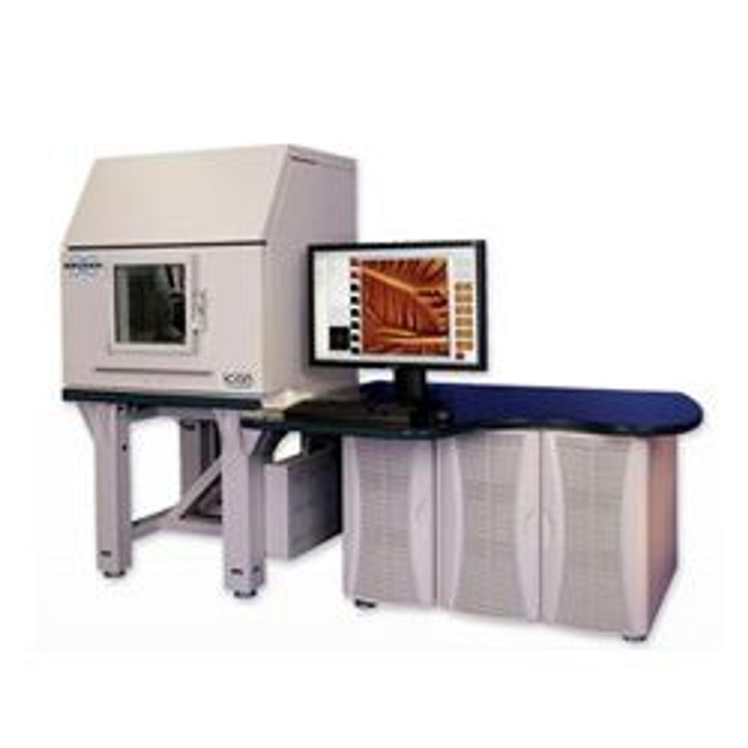
Dimension Icon Atomic Force Microscope
Bringing new levels of performance, functionality, and AFM accessibility to nanoscale researchers. The Dimension Icon® Atomic Force Microscope brings new levels of performance, functionality, and AFM accessibility to nanoscale researchers in science and industry. The culmination of decades of large-sample AFM technology, the system has been designed from top to bottom to deliver revolutionary low drift and low noise that allo…
The supplier does not provide quotations for this product through SelectScience. You can search for similar products in our Product Directory.
Great results
Materials morphology
Building upon the world’s most utilized large-sample AFM platform, it is the culmination of decades of technological innovation, customer feedback, and industry-leading application flexibility. The system has been designed from top to bottom to deliver the revolutionary low drift and low noise that allows users to achieve artifact-free images in minutes instead of hours.
Review Date: 1 Dec 2021 | Bruker Nano Surfaces and Metrology
Great results.
Materials
By combining the peak force tapping with electrochemical operation in liquid, in addition to surface topography, the electrochemical AFM can also provide corresponding mechanical, and electrochemical feature mapping of the sample. With all the advantages of EC-AFM, it can deliver excellent performance for in-situ analysis with nano-scale resolution of electrochemical cell during electrochemical reactions.
Review Date: 10 Feb 2020 | Bruker Nano Surfaces and Metrology
User friendly simple equipment.
Nanoscale surface studies
We have achieved reliable results. Very good platform.
Review Date: 23 Mar 2019 | Bruker Nano Surfaces and Metrology
We are very satisfied!
Semiconductor samples (SiO2, graphene, nanowires), polymeric samples
The Bruker ICON AFM system was installed four years ago in our clean room facility and it revealed as a unique instruments for its capability to perform low-noise and high-resolution imaging for many users, on many kind of samples and with reliable performances! “ScanAsyst” mode preserves the AFM probes in good condition for weeks and allow to any student to be independent and to start the measurements after a short training. We have also the Quantitative Nano machanics (QNM) module, taht allows to perform spatially resolved measurements od mechanical properties of the sample (stiffness, adhesion, dissipation, Young's module) in real time. From this point of vies the system is pretty unique, allowing to acquire for each single point a complete force-vs-distance curve.
Review Date: 12 Mar 2018 | Bruker Nano Surfaces and Metrology
Bringing new levels of performance, functionality, and AFM accessibility to nanoscale researchers.
The Dimension Icon® Atomic Force Microscope brings new levels of performance, functionality, and AFM accessibility to nanoscale researchers in science and industry. The culmination of decades of large-sample AFM technology, the system has been designed from top to bottom to deliver revolutionary low drift and low noise that allows users to achieve artifact-free images in minutes instead of hours.
The Icon is also equipped with proprietary ScanAsyst® automatic image optimization technology, which enables easier, faster, and more consistent results, regardless of user skill level. The Icon’s uncommon ease of use, ultimate performance, exceptional productivity, and superior versatility make it an ideal choice for practically every AFM application.
Dimension Icon Atomic Force Microscope Features:
- Proprietary sensor design achieves closed-loop performance with open-loop noise levels for previously unseen resolution on large-sample AFMs
- Significantly reduced noise floor enables imaging at atomic level in contact mode, with less than 30pm in TappingMode™
- Drift rates less than 200pm per minute render distortion-free images
- Integrated feedback alignment tools deliver quick and optimized probe positioning
- High-resolution camera and X-Y positioning permit faster, more efficient sample navigation
- ScanAsyst® Imaging and NanoScope® software with default experiment modes distill decades of knowledge into preconfigured settings
- Wide-open access to tip and sample accommodates a large variety of standard and customized experiments
- Instrument and software designed to take full advantage of all current and future Bruker AFM modes and techniques
- Custom user-programmable scripts offer semi-automated measurement and analysis