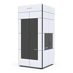
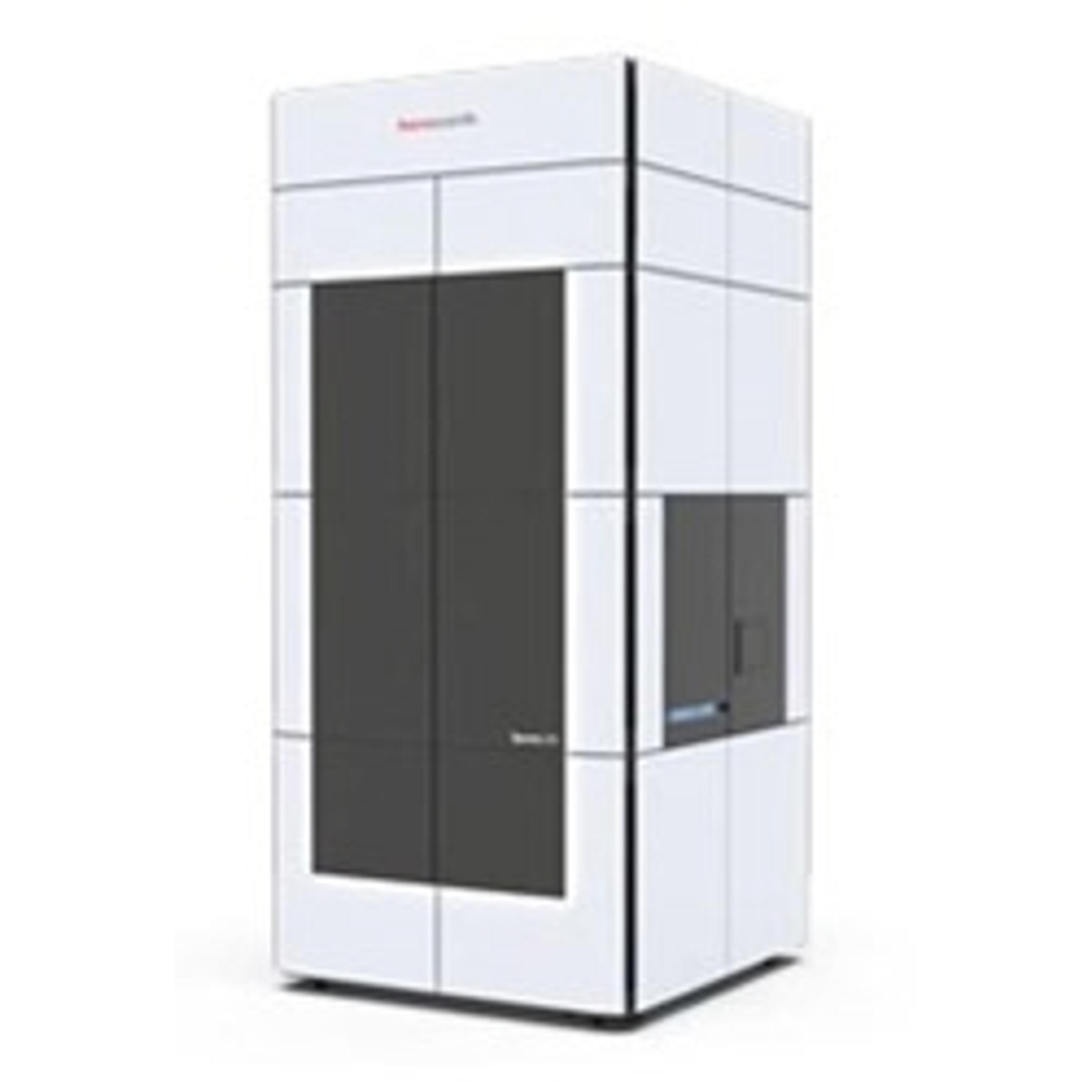
Spectra 300 TEM
High resolution TEM and STEM microscope for all materials science and semiconductor applications.

The supplier does not provide quotations for this product through SelectScience. You can search for similar products in our Product Directory.
As the fastest and most reliable instrument in its class, the Thermo Scientific™ Spectra 300 Scanning/Transmission Electron Microscope (S/TEM) provides unprecedented performance for the study of semiconductor materials and semiconductor failure analysis. Insight regarding advanced products, such as 7 nm or smaller node devices, is now within your grasp thanks to the unique combination of high-brightness field emission gun (X-FEG) and easy-to-use software. With its ability to generate fast EDS maps (without any loss of spatial resolution), as well as electron energy loss spectroscopy (EELS) and low-kV analysis, this is the ideal high-end S/TEM solution for industrial applications.
Key Benefits:
Unprecedented performance
Answer challenging questions in the advanced production of semiconductor devices, such as 7 nm or smaller node devices.
High-brightness FEG
Two high-brightness FEG options; the standard high-brightness field emission gun (X-FEG) or the optional high-brightness cold field emission gun (XCFEG). The X-FEG is suited for optimal performance, while the XCFEG is designed for ease-of-use (facilitating STEM, EELS and low-kV analysis).
Ease of use
With a robust suite of software and hardware tools designed to improve the user experience, the Spectra 300 S/TEM ensures efficient analysis and high productivity.


