
Application Notes
Resources
25
Selected Filters:
Application Notes
Hysitron PI Series PicoIndenters
Application Notes
Hysitron PI 89 SEM PicoIndenter
Application Notes
Mechanical characterization of ultra-low-k dielectric films
Application Notes
Strength engineering in a nickel-base superalloy
Application Notes
High-temperature investigation of a thermal barrier coating
White Papers
Multimodal correlative imaging of microplastics
Application Notes
In-situ mechanical testing of semiconductor devices
Application Notes
Targeted nanoindentation of a high-entropy alloy in the SEM
Application Notes
Hardness mapping of a DP980 steel sample
Application Notes
Improving additive manufacturing with accurate surface metrology
Application eBooks
Beyond the naked eye: Characterizing nanomaterials with precision
Today’s demand for faster and smaller electronics is ever growing. Discover how to meet this demand using the latest nanomaterial characterization techniques
Application Notes
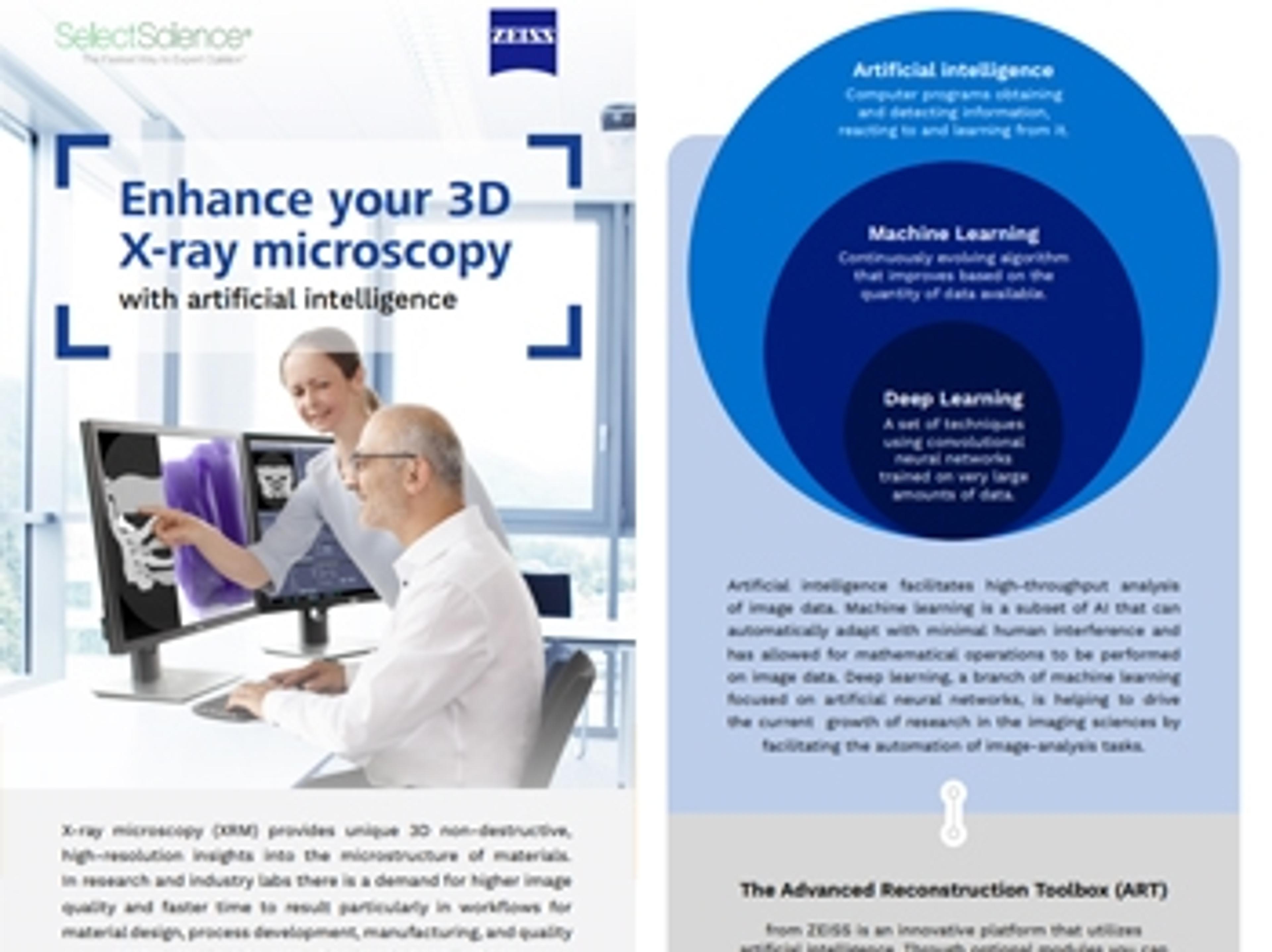
Enabling AI-based reconstruction for your ZEISS X-ray microscope
Product Brochures
Explore the ZEISS PhaseEvolve
Application Notes